Apparatus and method for test structure inspection

a technology of apparatus and structure, applied in electrical apparatus, electronic circuit testing, instruments, etc., can solve the problems of compromising sensitivity, limiting the amount of current that can be injected into individual device features, and failure to apply focussing ion beam cross sectioning only

Active Publication Date: 2011-03-08
APPL MATERIALS ISRAEL LTD
View PDF17 Cites 80 Cited by
  • Summary
  • Abstract
  • Description
  • Claims
  • Application Information

AI Technical Summary

Problems solved by technology

However, when an electrical error is detected it is only localized to a somewhat large area on the test chip.
This means that a failure technique such as focused ion beam cross sectioning can only be applied if the defect is further localized by a following technique such as ADL™.
As the device scale shrinks to 45 nm technology and beyond, the amount of current that can be injected into an individual device feature becomes limited.
In both cases, these are resistive defects and the capacitance of the structure is not of interest.
In these cases, if the exposure time is short relative to the RC response of the structure with capacitance C containing a defect with capacitance R, the sensitivity will be compromised.

Method used


Image

  • Apparatus and method for test structure inspection
  • Apparatus and method for test structure inspection
  • Apparatus and method for test structure inspection

Examples


Embodiment Construction

[0016]Reference will now be made in detail to an implementation consistent with the present invention as illustrated in the accompanying drawings. Wherever possible, the same reference numbers will be used throughout the drawings and the following description to refer to the same or like parts. Although discussed with reference to these illustrations, the present invention is not limited to the implementations illustrated therein. Hence, the reader should regard these illustrations merely as examples of embodiments of the present invention, the full scope of which is measured only in terms of the claims following this description.

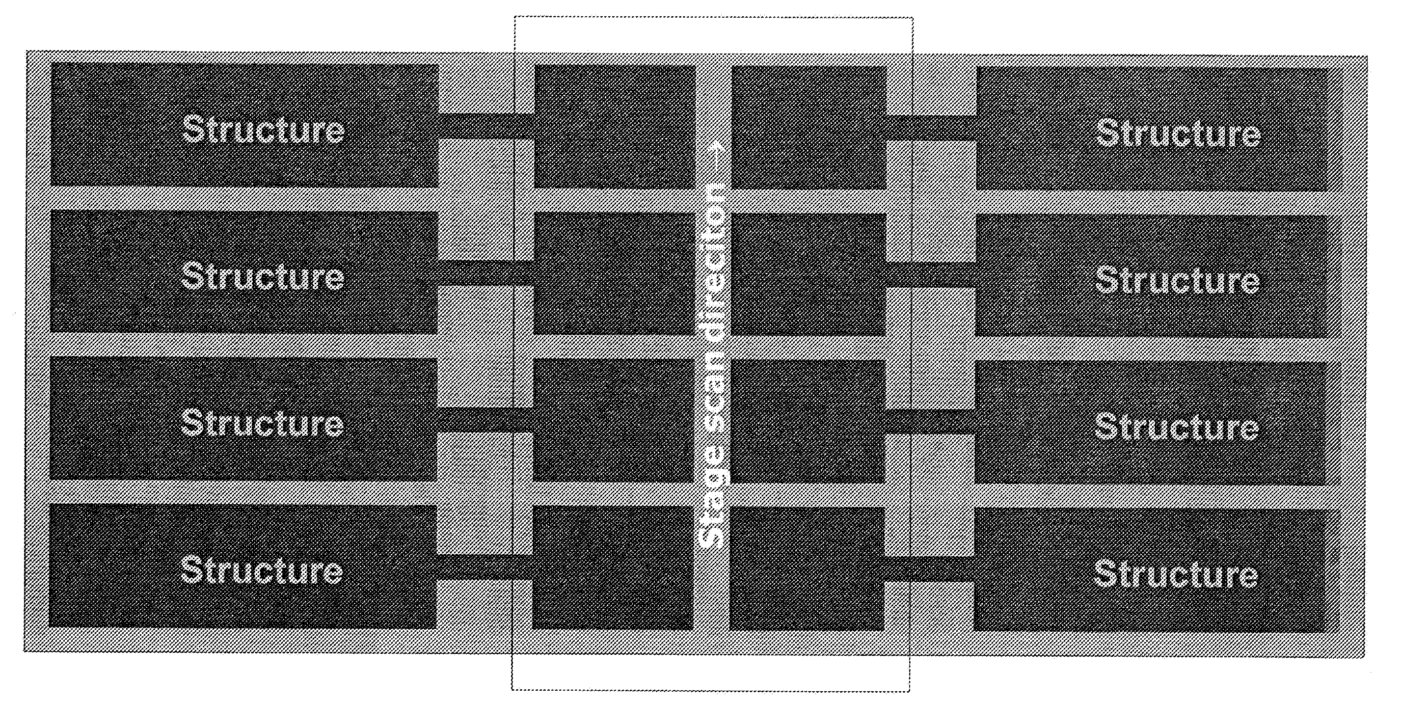
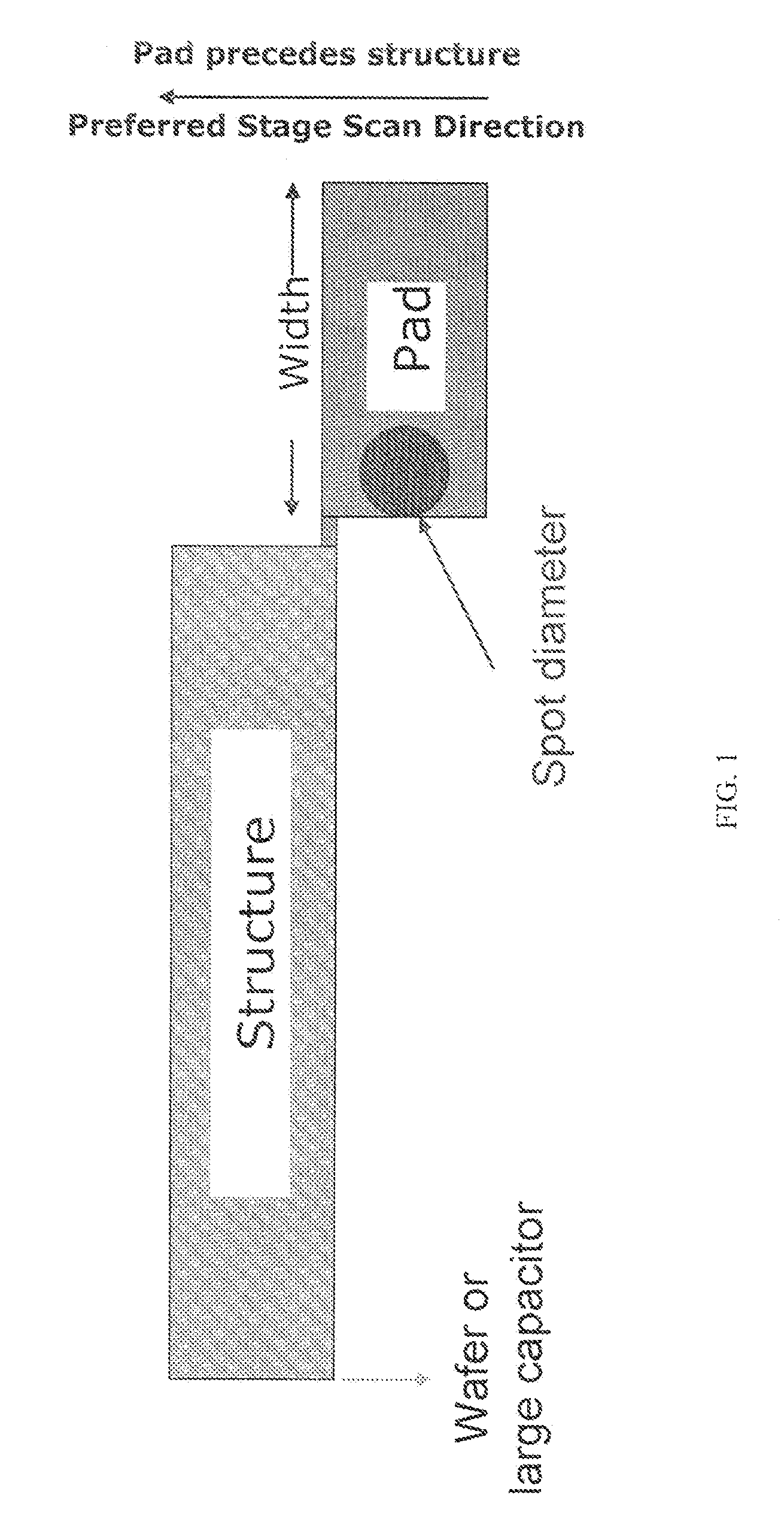
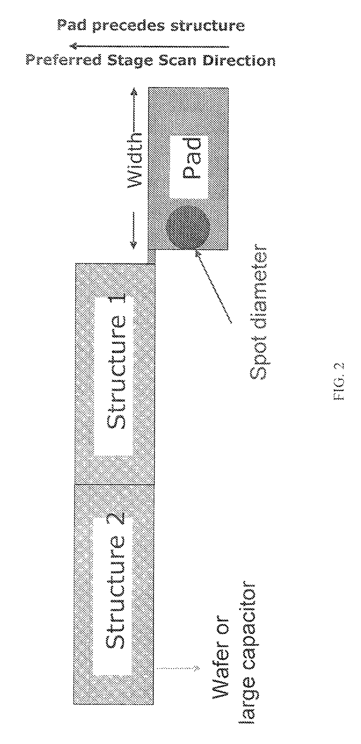
[0017]In one embodiment of the invention, a conducting pad is electrically connected to the structure under test as shown in FIG. 1. In one instance, the pad end of the structure is floating and the opposite end is electrically connected to the wafer. In another instance, both ends are floating and the end opposite the pad is connected to a large capacitanc...


PUM


Abstract

Herein are described layouts of test structures and scanning methodologies that allow large probe currents to be used so as to allow the detection of resistive defects with a resistance lower than 1 MΩ while at the same time allowing a sufficient degree of localization to be obtained for root cause failure analysis. The detection of resistances lower than 1 MΩ nominally requires a probe current greater than 1 micro ampere for detection on an electron beam inspection system.

Description

RELATED APPLICATIONS[0001]This application claims the benefit of U.S. Provisional Application No. 60 / 755,942, filed Jan. 3, 2006, which is incorporated herein by reference.FIELD OF THE INVENTION[0002]This invention relates to apparatus and methods for inspecting and testing semiconductor wafers during circuit fabrication.BACKGROUND OF THE INVENTION[0003]Test structures are often utilized in the semiconductor device industry as a method for rapidly developing a process flow. Many existing methodologies currently exist such as KLA Tencor's uLoop™, Applied Material's, Inc. ADL™ and the Real Vision™ jointly developed by Applied Materials Inc. and PDF Solutions Inc. These techniques allow a large number of devices to be rapidly tested allowing determination of root cause failure analysis in a relatively short period of time.[0004]There are two basic requirements of any such technique to be useful for rapid diagnostics and root cause failure analysis. These are 1) detection of the electri...

Claims


Application Information

Patent Timeline
Patent Type & Authority Patents(United States)
IPC IPC(8): G01R31/305
CPCG01R31/2884H01L22/14G01R31/305
Inventor BULLOCK, EUGENE T.
Owner APPL MATERIALS ISRAEL LTD
Why Eureka
Try Eureka