Nonvolatile semiconductor memory device and fabrication method therefor

a semiconductor memory and non-volatile technology, applied in semiconductor devices, transistors, instruments, etc., can solve problems such as deterioration of charge retaining capacity, and achieve the effects of reducing voltage, good data retaining characteristic, and high charge injection efficiency

Inactive Publication Date: 2011-04-05
SONY CORP
View PDF5 Cites 6 Cited by
  • Summary
  • Abstract
  • Description
  • Claims
  • Application Information

AI Technical Summary

Benefits of technology

[0017]Therefore, it is demanded to provide a nonvolatile semiconductor memory device which is high in charge injection efficiency and which allows a further reduction of the voltage.
[0020]According to another embodiment of the present invention, there is provided a nonvolatile semiconductor memory device including a memory transistor. The memory transistor has a channel formation region defined between two source and drain regions formed on a semiconductor substrate, a bottom insulating film, a charge storage film and a top insulating film formed in order at least on the channel formation region, the charge storage film having a charge storage function, and a gate electrode formed on the top insulating film. The bottom insulating film is formed from a film of a single layer containing nitrogen such that the content of nitrogen with respect to silicon in a lowermost layer region of the film which contacts with the channel formation region and an uppermost layer region of the film which contacts with the gate electrode is higher than that of the other film region or regions which exist between the uppermost and lowermost regions.
[0026]According to a still further embodiment of the present invention, there is provided a nonvolatile semiconductor memory device including a memory transistor. The memory transistor has a channel formation region defined between two source and drain regions formed on a semiconductor substrate, a bottom insulating film, a charge storage film and a top insulating film formed in order at least on the channel formation region, the charge storage film having a charge storage function, and a gate electrode formed on the top insulating film. The bottom insulating film is formed from a film of a single layer such that a barrier energy with respect to silicon of a lowermost layer region of the film which contacts with the channel formation region and an uppermost layer region of the film which contacts with the gate electrode is lower than that of the other film region or regions which exist between the uppermost and lowermost regions.
[0029]Preferably, the barrier energy of the bottom insulating film with respect to silicon is lower than that of silicon oxide with respect to silicon.

Problems solved by technology

If a local leak current path is produced by a defect or the like in the bottom insulating film, then in a FG type memory transistor, most of the stored charge leaks to the substrate side along the leak path, resulting in deterioration of the charge retaining capacity.

Method used


Image

  • Nonvolatile semiconductor memory device and fabrication method therefor
  • Nonvolatile semiconductor memory device and fabrication method therefor
  • Nonvolatile semiconductor memory device and fabrication method therefor

Examples


Embodiment Construction

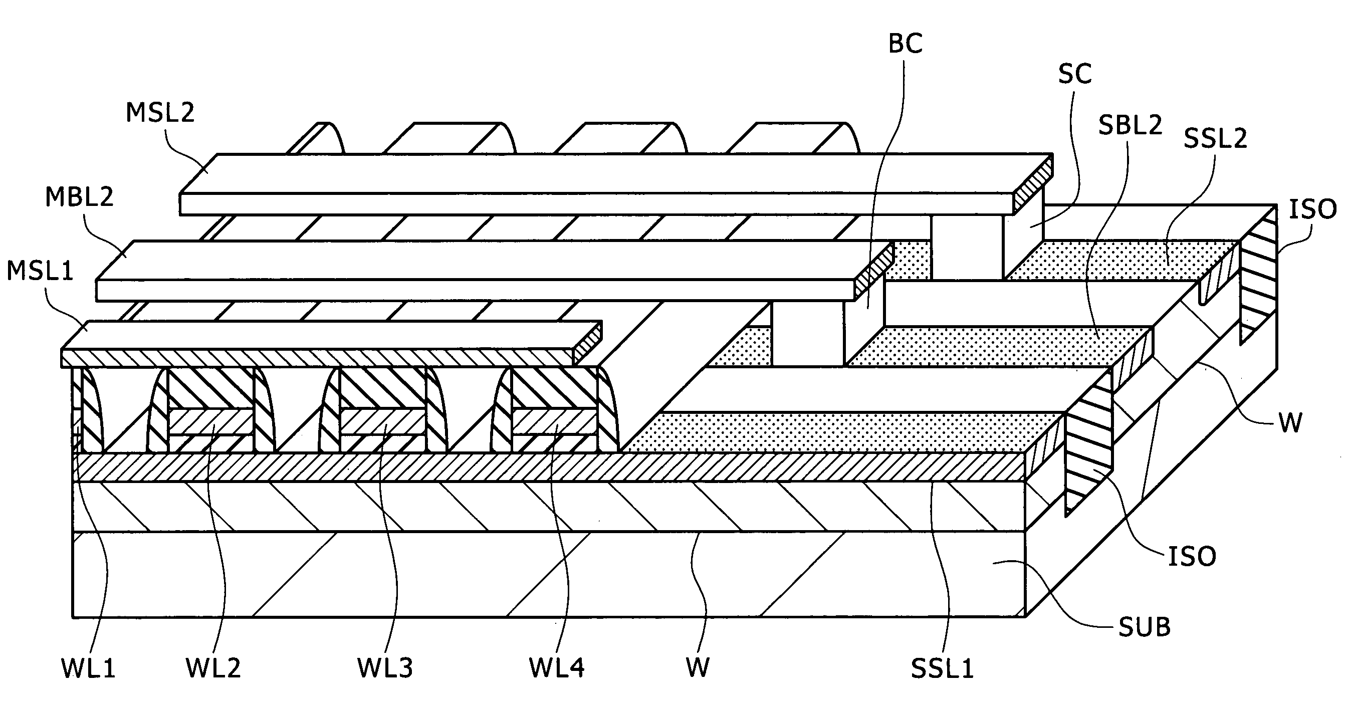
[0050]In the following, a preferred embodiment of the present invention is described wherein the present invention is applied to a nonvolatile memory device which uses a MONOS type memory transistor.

>

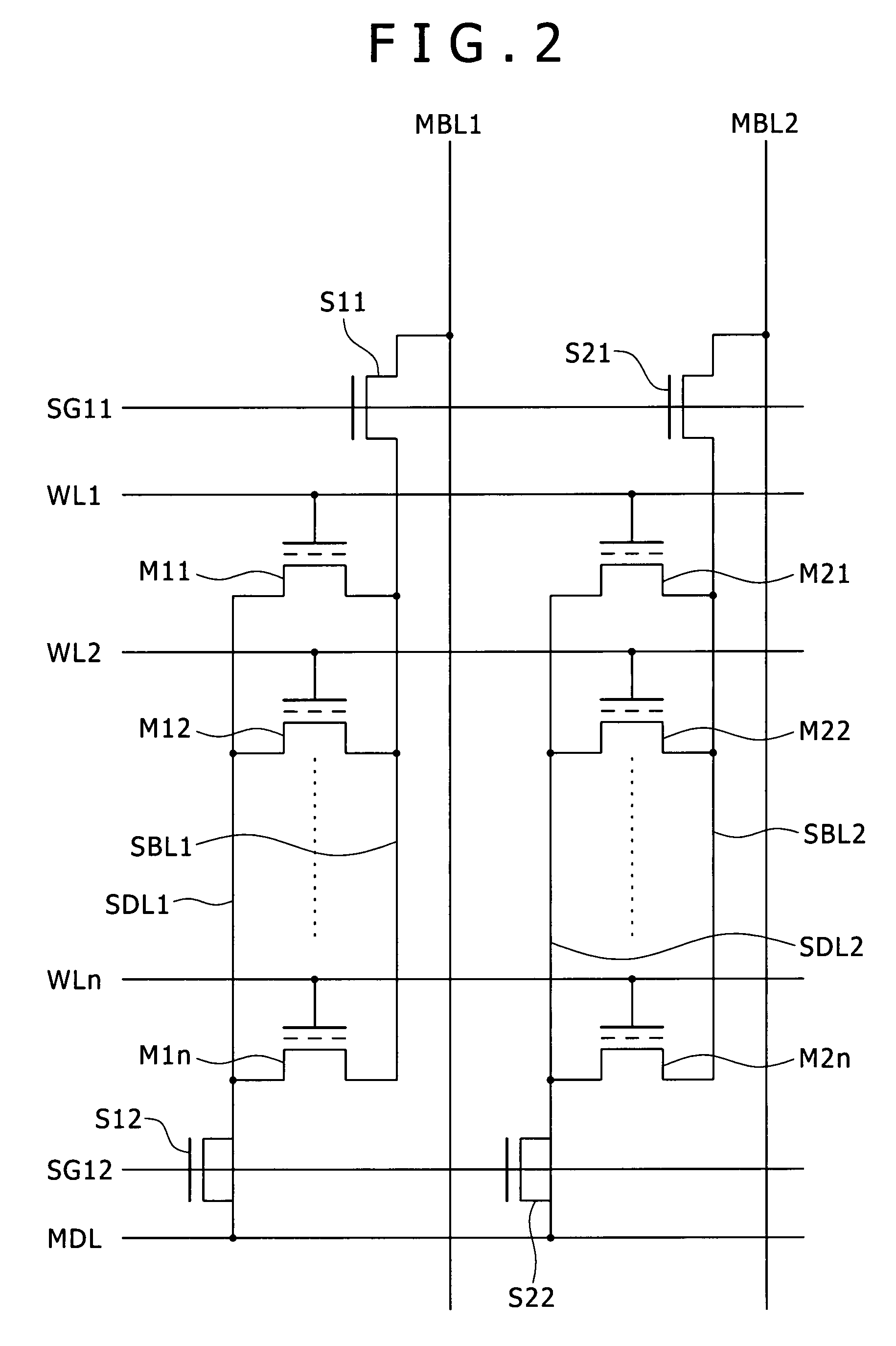
[0051]The nonvolatile memory device according to the present embodiment includes a memory block and a logic circuit block.

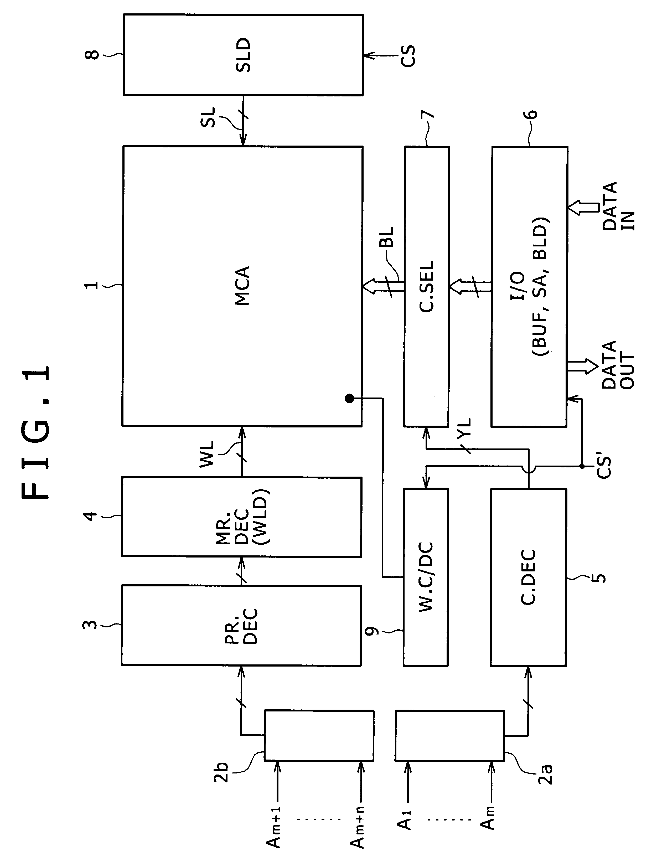
[0052]FIG. 1 shows a general configuration of the memory block.

[0053]Referring to FIG. 1, the memory block shown includes a memory cell array (MCA) 1 and memory peripheral circuits for controlling operation of the memory cell array 1. The memory peripheral circuits can output at least ±4 V as a maximum voltage.

[0054]The memory peripheral circuits include a column buffer 2a, a row buffer 2b, a pre-row decoder (PR.DEC) 3, a main row decoder (MR.DEC) 4, a column decoder (C.DEC) 5, an input / output circuit (I / O) 6, a column gate array (C.SEL) 7, a source line driving circuit (SLD) 8 and a well charge / discharge circuit (W.C / DC) 9. Though not particularly shown, the memory ...


PUM


Abstract

Disclosed herein is a nonvolatile semiconductor memory device, including a memory transistor. The memory transistor has a channel formation region defined between two source and drain regions formed on a semiconductor substrate a bottom insulating film, a charge storage film and a top insulating film formed in order at least on the channel formation region, the charge storage film having a charge storage function, and a gate electrode formed on the top insulating film. The bottom insulating film is formed from a plurality of films containing nitrogen such that the content of nitrogen of a lowermost one of the films which contacts with the channel formation region and an uppermost one of the films which contacts with the gate electrode is higher than that of the other one or ones of the films which exist between the uppermost and lowermost films.

Description

CROSS REFERENCES TO RELATED APPLICATIONS[0001]The present invention contains subject matter related to Japanese Patent Application JP 2006-225140, filed in the Japan Patent Office on Aug. 22, 2006, the entire contents of which are incorporated herein by reference.BACKGROUND OF THE INVENTION[0002]1. Field of the Invention[0003]This invention relates to a nonvolatile semiconductor memory device wherein a memory transistor includes a channel formation region, a gate electrode and a charge storage film disposed between the channel formation region and the gate electrode and having a charge storage function and also to a fabrication method for the nonvolatile semiconductor memory device.[0004]2. Description of the Related Art[0005]Nonvolatile semiconductor memory transistors can be roughly classified into a floating gate (FG) type and a metal-oxide-nitride-oxide semiconductor (MONOS) type. In a nonvolatile semiconductor transistor of the FG TYPE, a charge storage section (floating gate) ...

Claims


Application Information

Patent Timeline
Patent Type & Authority Patents(United States)
IPC IPC(8): H01L29/76
CPCB82Y10/00G11C16/0466H01L21/28282H01L29/792H01L27/11568H01L29/42348H01L29/66833H01L27/115G11C2216/06H01L29/40117H10B43/30H10B69/00
Inventor FUJIWARA, ICHIROAOZASA, HIROSHI
Owner SONY CORP
Why Eureka
Try Eureka