Electronic device, image display device and sensor, and method for manufacturing electronic device

a technology of image display and electronic devices, applied in the direction of thermoelectric devices, sustainable manufacturing/processing, final product manufacturing, etc., can solve the problems of reducing the reliability of tft, and achieve the effect of improving the efficiency of charge injection

Active Publication Date: 2015-09-03
SONY CORP
View PDF1 Cites 14 Cited by
  • Summary
  • Abstract
  • Description
  • Claims
  • Application Information

AI Technical Summary

Benefits of technology

[0054]In the method for manufacturing an electronic device according to the first aspect or third aspect of the present disclosure, the electrode modification material contained in the active layer is diffused into the first electrode and the second electrode to modify, with the electrode modification material, the portions of the first electrode and second electrode in contact with the active layer. In addition, in the method for manufacturing an electronic device according to the second aspect or fourth aspect of the present disclosure, the electrode modification material attached to the surface of the active layer is reacted with the first electrode and the second electrode to modify, with the electrode modification material, the portions of the first electrode and second electrode in contact with the active layer. Furthermore, in the electronic device according to the first aspect or second aspect of the present disclosure, and the electronic device constituting the image display device or sensor according to the present disclosure, the portions of the first electrode and second electrode in contact with the active layer are modified with the electrode modification material. Accordingly, it becomes possible to improve the charge injection efficiency without causing any problems with adhesion and selectivity, reliability, or the like between the organic semiconductor layer and the source / drain electrodes.

Problems solved by technology

However, the bottom-contact structure has, due to differences in mechanical characteristic value between the source / drain electrodes and the channel forming region, problems such as difficulty in controlling strain caused at the interface on flexion or on heating, thereby leading to decreased reliability of the TFT.

Method used


Image

  • Electronic device, image display device and sensor, and method for manufacturing electronic device
  • Electronic device, image display device and sensor, and method for manufacturing electronic device
  • Electronic device, image display device and sensor, and method for manufacturing electronic device

Examples


example 1

[0104]Example 1 relates to a method for manufacturing an electronic device according to the first aspect of the present disclosure, and an electronic device according to the first aspect of the present disclosure, as well as an image display device.

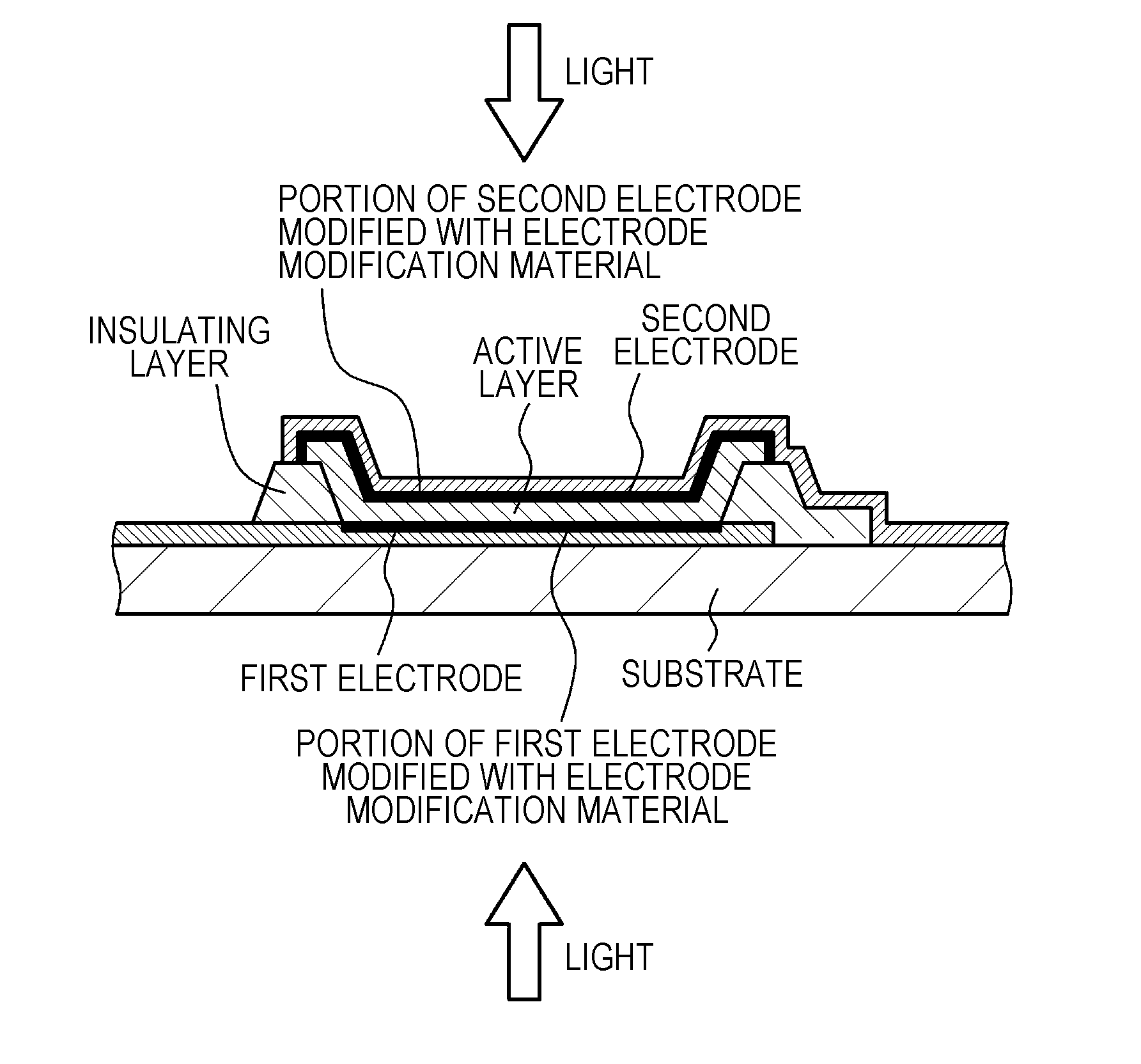
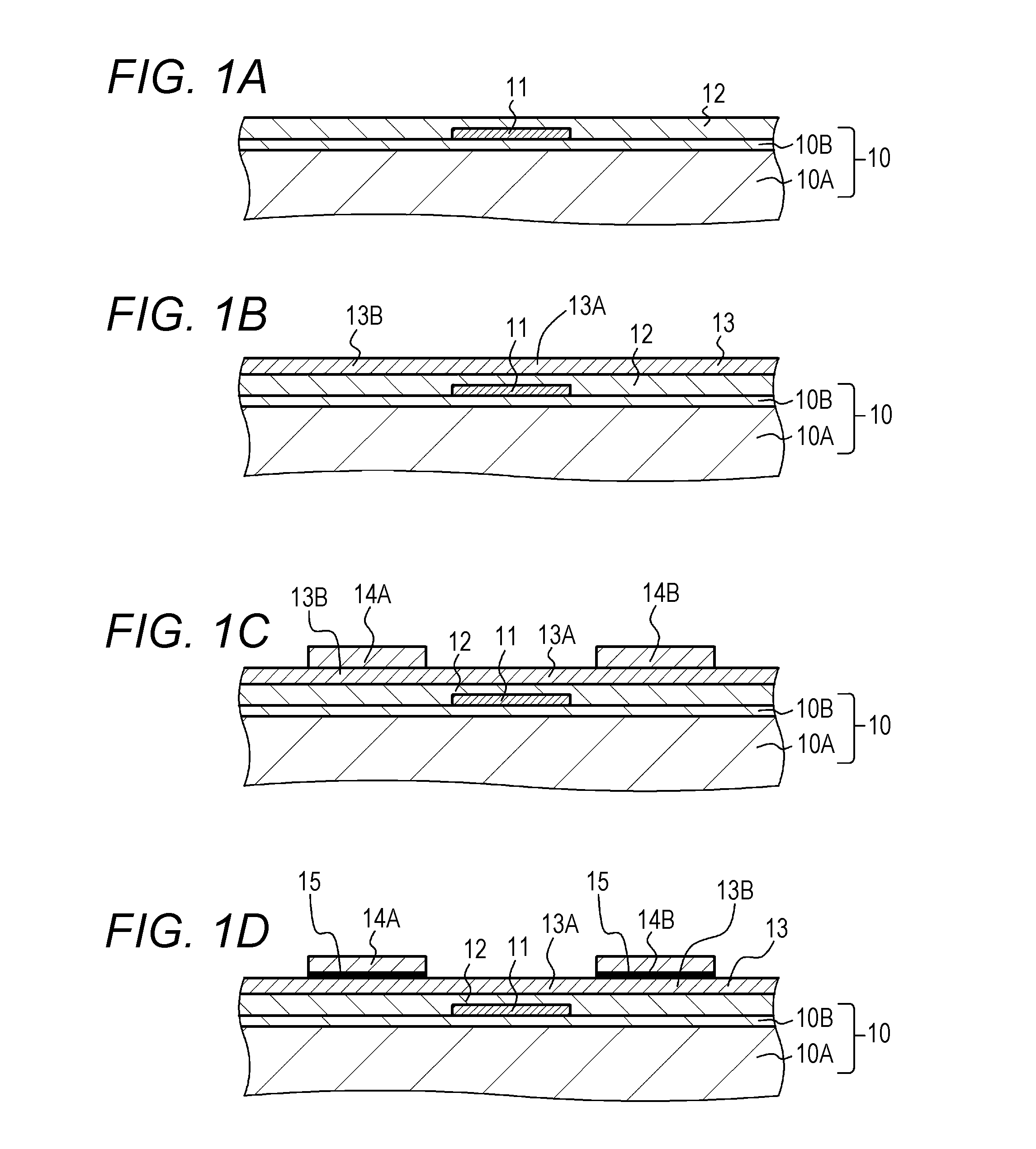
[0105]The electronic device of Example 1 of a bottom gate / top contact type is a three-terminal electronic device, specifically, a TFT, which is an electronic device including: as in the schematic partial cross-sectional view shown in FIG. 1D,

[0106](a) a control electrode 11 formed on a substrate 10;

[0107](b) an insulating layer 12 covering the control electrode 11;

[0108](c) an active layer 13 including an organic semiconductor material, which is formed on the insulating layer 12; and

[0109](d) a first electrode 14A and a second electrode 14B formed on the active layer 13,

[0110]where portions of the first electrode 14A and second electrode 14B in contact with the active layer 13 are modified with an electrode modification material.

[0111]It ...

example 2

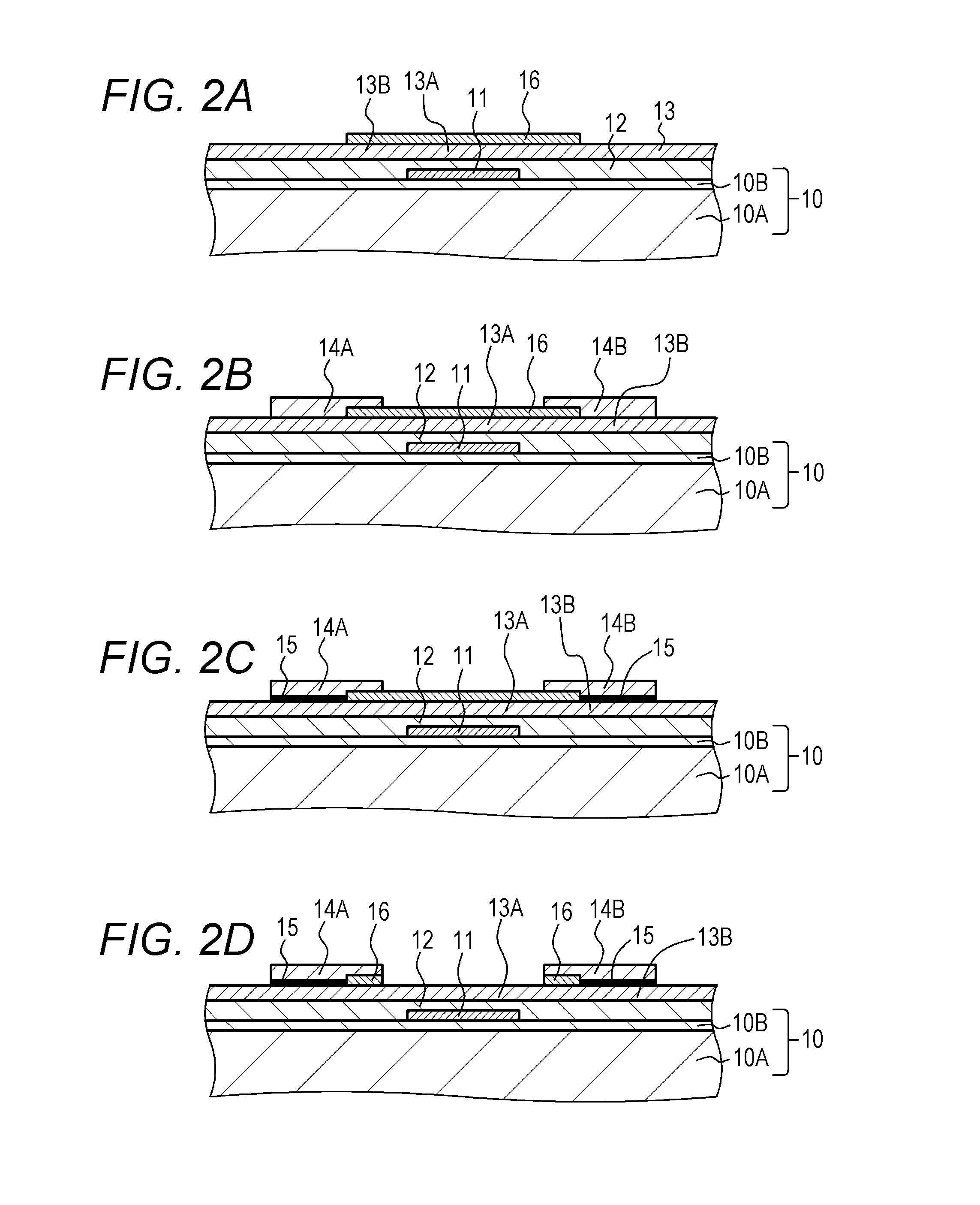
[0128]Example 2 is a modification of Example 1. A method for manufacturing a three-terminal electronic device (bottom gate / top contact TFT) of Example 2 will be described below with reference to FIGS. 2A, 2B, 2C, and 2D which are schematic partial cross-sectional views of a substrate and the like.

Step-200

[0129]First, similar steps as the [Step-100] through [Step-110] in Example 1 are executed.

Step-210

[0130]Next, a protective film 16 is formed over a portion of the active layer 13. Specifically, in accordance with a CVD method, the protective film 16 including a silicon oxide film is formed over the channel forming region 13A and over a portion of the channel forming region extension 13B (see FIG. 2A).

Step-220

[0131]Thereafter, the source / drain electrodes 14A, 14B are formed on the active layer 13 (specifically, on the channel forming region extension 13B) and the protective film 16. Specifically, the step is executed in similar way as in the [Step-120] in Example 1 (see FIG. 2B), and...

example 3

[0133]Example 3 relates to a method for manufacturing an electronic device according to the second aspect of the present disclosure, and an electronic device according to the first aspect of the present disclosure, as well as an image display device. The electronic device of Example 3 of a bottom gate / top contact type is a three-terminal electronic device, specifically, a TFT, which has largely similar configuration and structure as shown in FIG. 1D.

[0134]It is to be noted that the electrode modification material includes a thiol, specifically, tetrafluorobenzenethiol in Examples 3 to 4, Examples 7 to 8, and Example 9. Moreover, portions of the source / drain electrodes 14A, 14B in contact with the channel forming region extension 13B are modified with the electrode modification material, and the material constituting the source / drain electrodes 14A, 14B reacts with the electrode modification material in the portions of the source / drain electrodes 14A, 14B, which are modified with the...


PUM


Abstract

An electronic device includes a control electrode 11 formed on a substrate 10, an insulating layer 12 covering the control electrode 11, an active layer 13 including an organic semiconductor material, which is formed on the insulating layer 12, and a first electrode 14A and a second electrode 14B formed on the active layer 13, and portions 15 of the first electrode and second electrode in contact with the active layer 13 are modified with an electrode modification material.

Description

TECHNICAL FIELD[0001]The present disclosure related to an electronic device, an image display device and a sensor, a method for manufacturing an electronic device.BACKGROUND ART[0002]In the case of a bottom-gate TFT as a type of organic thin film transistor (organic TFT), two types of electrode structures are known, such as a top-contact structure with source / drain electrodes formed on a channel forming region including an organic semiconductor layer and a bottom-contact structure with source / drain electrodes formed below a channel forming region (see, for example, Advanded Materials vol. 14, p. 99 (2002), C. D. Dimitrakopoulos, et al.). Furthermore, also in the case of a top-gate TFT, two types of electrode structures are known, such as a top-contact structure with source / drain electrodes formed on a channel forming region and a bottom-contact structure with source / drain electrodes formed below a channel forming region.[0003]In the case of the bottom-contact structure, high-definit...

Claims


Application Information

Patent Timeline
Patent Type & Authority Applications(United States)
IPC IPC(8): H01L29/40H01L21/283H01L51/56H01L51/00H01L51/50H01L27/15H01L21/02
CPCH01L29/408H01L27/153H01L21/283H01L51/56H01L51/0002H01L51/0021H01L51/50H01L21/02107Y02E10/549Y02P70/50H10K10/466H10K10/84H10K59/00H10K30/81H10K30/88H10K50/00H10K50/844H10K71/00H10K71/10H10K71/60
Inventor KATSUHARA, MAOONO, HIDEKIUSHIKURA, SHINICHIISHII, YUI
Owner SONY CORP
Why Eureka
Try Eureka