Semiconductor device

a technology of semiconductor devices and semiconductors, applied in semiconductor devices, semiconductor/solid-state device details, electrical apparatus, etc., can solve the problems of inability to produce stable devices, short circuit between adjacent connecting plugs, and similar problems, and achieve effective inhibition, increase center-to-center distance, and improve the production yield of semiconductor devices

Active Publication Date: 2011-05-03
RENESAS ELECTRONICS CORP
View PDF10 Cites 1 Cited by
  • Summary
  • Abstract
  • Description
  • Claims
  • Application Information

AI Technical Summary

Benefits of technology

[0017]This configuration can provide an increased center-to-center distance of the second plugs, such that a pair of second plugs can stably be formed in the thick second interlayer insulating film in mutually separated arrangement, even if a pair of adjacent connecting plugs are closely provided. In addition, the configuration can also provide an effective inhibition of a failure in the manufacture such as a short-circuit between the connecting plugs and the like. Thus, according to the present invention, an improved production yield of the semiconductor devices can be achieved.
[0022]On the contrary, in the present invention, the first plug and the second plug are arranged so that a center-to-center distance of the second plugs that extends through the third interlayer insulating film and the fourth interlayer insulating film is larger than a center-to-center distance of the first plugs that extends through the first interlayer insulating film, in the pair of adjacent second connecting plugs. This allows providing an increased center-to-center distance of the second plugs that extends through a capacitor-forming layer and an interlayer insulating film disposed above the capacitor-forming layer. Therefore, a pair of second plugs can stably be formed in mutually separated arrangement, even if the pair of adjacent connecting plugs are closely disposed. In addition, the configuration can also provide an effective inhibition of a failure in the manufacture such as a short-circuit between the second connecting plugs and the like. Thus, according to the present invention, an improved production yield of the semiconductor devices can be achieved.
[0023]Since the first plug and the second plug are arranged so that the center-to-center distance of the second plugs is larger than the center-to-center distance of the underlying first plugs according to the present invention as described above, a stable formation of a plurality of stacked contacts in closer locations can be achieved.

Problems solved by technology

However, the present inventor has investigated and found problems.
A progressing miniaturization of devices requires a reduced space between the stack contacts, and in such environment, a stable formation may be often difficult, when a plurality of connecting plugs that extends through a capacitor-forming layer and an interlayer insulating film disposed thereon are formed to be arranged in mutually adjacent relationship.
When a miniaturization is further progressed, it is concerned that such problem may leads to cause a short circuit between adjacent connecting plugs.
While the devices having the DRAM capacitor have been illustrated in the above description, similar problems may also be occurred when a relatively bulky element such as a capacitor and the like is formed in an interlayer insulating film.
In other words, since a thickness of the interlayer insulating film is increased in a region for forming a relatively bulky element, it may often be difficult to form a pair of adjacent connecting plugs extending beyond such interlayer insulating film to the upper layer thereof.
When a pair of adjacent second connecting plugs are provided to be mutually closer arrangement in the conventional technology, a stable formation of the second plug may be often difficult, as described above.

Method used


Image

  • Semiconductor device
  • Semiconductor device
  • Semiconductor device

Examples


first embodiment

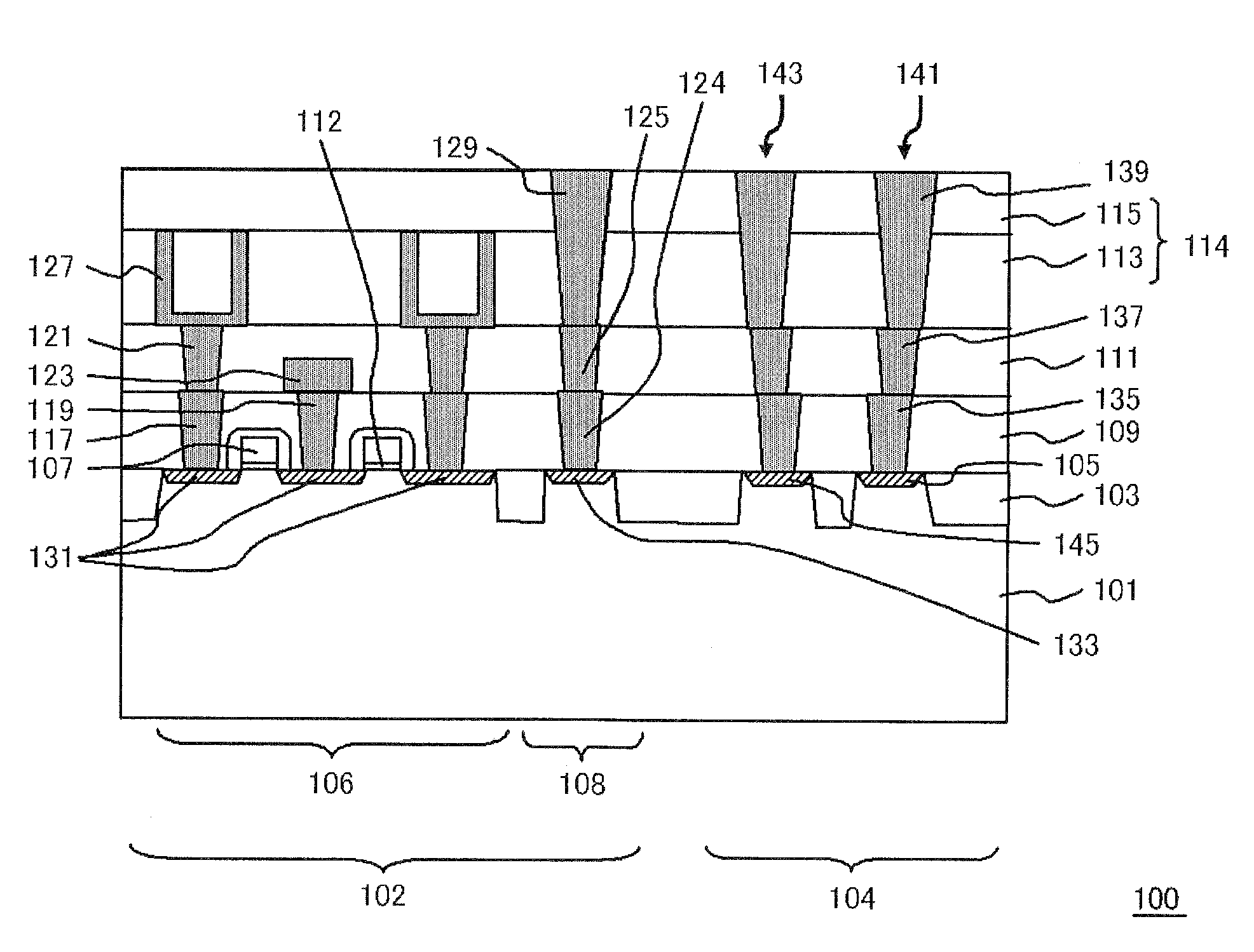
[0035]FIG. 1 is a cross-sectional view, illustrating a configuration of a semiconductor device of the present embodiment.

[0036]A semiconductor device 100 shown in FIG. 1 includes a first interlayer insulating film 109 provided above a semiconductor substrate (silicon substrate 101), and a second interlayer insulating film 114 provided above the first interlayer insulating film 109 and having larger thickness than the first interlayer insulating film 109.

[0037]In the present embodiment, the second interlayer insulating film 114 is composed of a third interlayer insulating film 113 provided above the first interlayer insulating film 109 and a fourth interlayer insulating film 115 provided so as to be in contact with an upper side of the third interlayer insulating film 113, and the third interlayer insulating film 113 is thicker than the first interlayer insulating film 109. However, the second interlayer insulating film 114 is not limited to a multiple-layered film, and may also be c...

second embodiment

[0075]In the semiconductor device of first embodiment (FIG. 1), a misalignment may be created between the plug of the upper layer and the plug of the lower layer, which constitute a stack contact. In the present embodiment, an example of causing a misalignment will be described.

[0076]FIG. 3 is a cross-sectional view, illustrating a configuration of a semiconductor device of the present embodiment. The fundamental configuration of the semiconductor device shown in FIG. 3 is similar to that shown in FIG. 1, except that a misalignment is caused between the plug 137 and the plug 139.

[0077]When a misalignment is caused in a conventional device, all of the adjacent plugs 139 are formed to be equally moved toward the same direction in the surface, and the center-to-center distance itself of the plugs 139 is not changed. Thus, there is a concern that a formation failure of the plugs 139 described above is caused regardless of conducting an alignment.

[0078]On the contrary, since the center-t...

third embodiment

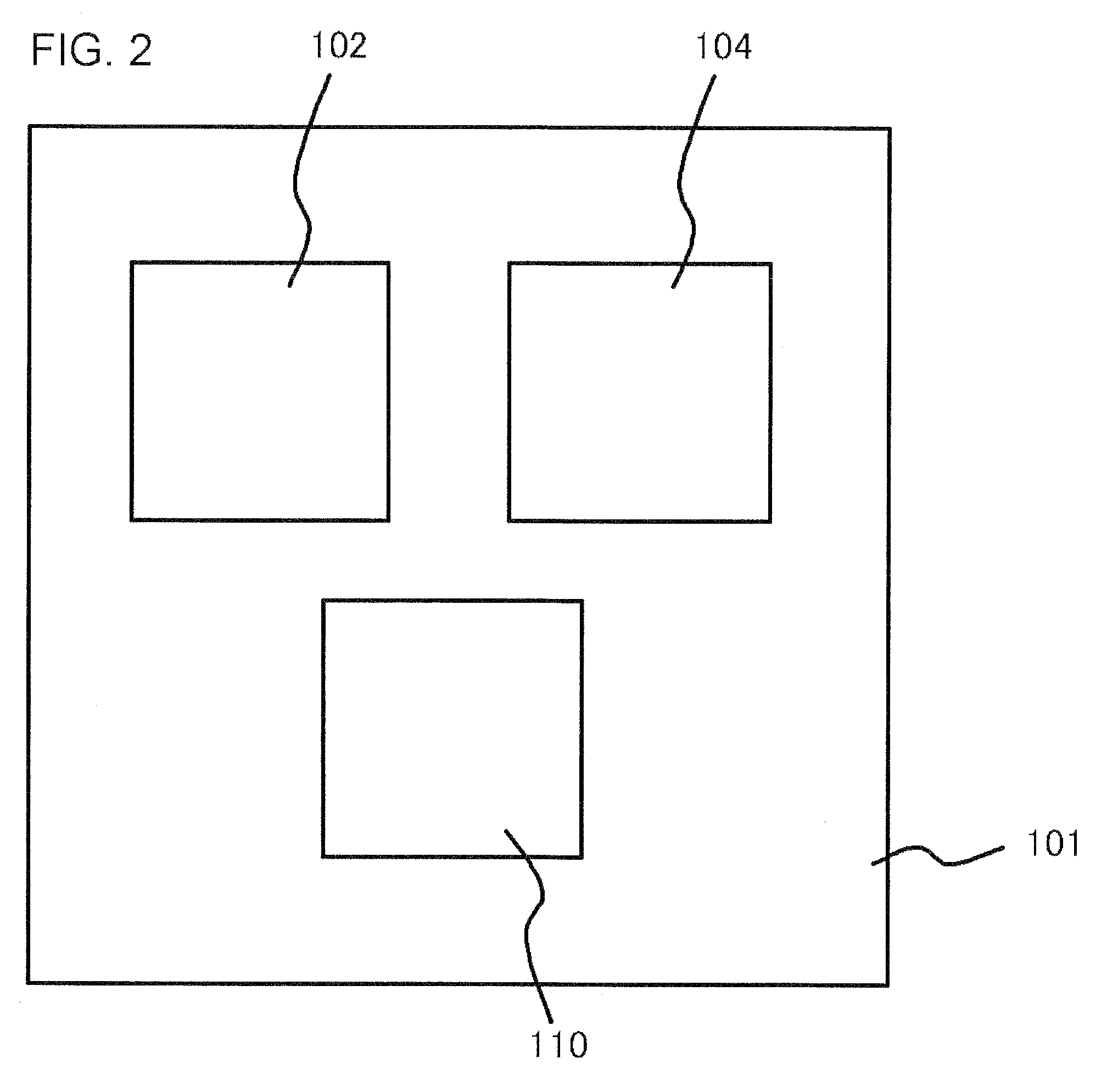
[0081]In the semiconductor devices as described in the above-mentioned embodiments, the stack contact 141 and the stack contact 143 may alternatively be an ordinary contact plug of the SRAM cell.

[0082]FIG. 4 is a plan view, illustrating a configuration of a SRAM unit 104 of a semiconductor device according to the present embodiment. Here, a configuration of an unit cell in the SRAM will be illustrated. The unit cell includes a semiconductor region (p+ diffusion layer region, however n− channel region beneath gate electrode) 155 and a semiconductor region (p+ diffusion layer region, however n− channel region beneath gate electrode) 153, which are formed in a n-well (not shown), a semiconductor region (n+ diffusion layer region, however p− channel region beneath gate electrode) 157 and a semiconductor region (n+ diffusion layer region, however p− channel region beneath gate electrode) 151, which are formed in a p-well (not shown), and an element isolation region 103 (FIG. 4, not shown...


PUM


Abstract

In a pair of adjacent stack contact and stack contact in the semiconductor device, the plugs and the plugs are disposed so that a center-to-center distance of the plugs extending through a second interlayer insulating film, which is thicker than the first interlayer insulating film, is larger than a center-to-center distance of the plugs extending through the first interlayer insulating film.

Description

[0001]This application is based on Japanese patent application No. 2006-242,761, the content of which is incorporated hereinto by reference.BACKGROUND[0002]1. Technical Field[0003]The present invention relates to a semiconductor device, and in particular relates to a semiconductor device having a stack contact, in which a plurality of plugs are stacked.[0004]2. Related Art[0005]Typical conventional technologies related to semiconductor devices having a stack-type dynamic random access memory (DRAM) capacitor includes technologies disclosed in Japanese Patent Laid-Open No. 2002-203,812, Japanese Patent Laid-Open No. 2002-353,334 and Japanese Patent Laid-Open No. 2003-23,111. Among these, Japanese Patent Laid-Open No. 2002-203,812 discloses a technology of forming contact holes of a stacked structure in a semiconductor device, which compatibly contains DRAM cell and a logic embedded therein.[0006]On the other hand, Japanese Patent Laid-Open No. 2002-353,334 discloses a semiconductor d...

Claims


Application Information

Patent Timeline
Patent Type & Authority Patents(United States)
IPC IPC(8): H01L27/108H01L29/94
CPCH01L21/76816H01L23/485H01L27/105H01L27/10894H01L27/11H01L27/1116H01L2924/0002H01L2924/00H10B12/09H10B10/18H10B10/00
Inventor OHNO, AKIO
Owner RENESAS ELECTRONICS CORP
Why Eureka
Try Eureka