Method of MRAM fabrication with zero electrical shorting

a technology of random access memory and fabrication method, which is applied in the direction of magnetic field-controlled resistors, digital storage, instruments, etc., can solve the problems of electrical shorting, mtj etching is perhaps the most troublesome step in providing a limitation on shorting, and short current around the junction, so as to reduce or eliminate electrical shorting in the resulting cell

Active Publication Date: 2011-05-03
TAIWAN SEMICON MFG CO LTD
View PDF15 Cites 71 Cited by
  • Summary
  • Abstract
  • Description
  • Claims
  • Application Information

AI Technical Summary

Benefits of technology

[0019]A first object of this invention is to provide a method for RIE patterning of an MTJ stack (such as described above) that substantially reduces or eliminates electrical shorting in the resulting cell.
[0020]A second object of this invention is to provide a method for RIE patterning of an MTJ stack that does not result in the creation of unetched footings around the base of the patterned stack.
[0021]A third object of the present invention is to provide a method for RIE patterning of an MTJ stack that does not result in the re-deposition of etching residue about the base of the stack.
[0022]A fourth object of the present invention is to provide a method of eliminating large standard deviations in the of distributions of sensor resistances.
[0032]5. in another chamber, etch the remaining unetched layers using a CH3 OH etchant under high bias power, during which process the remaining Ta hard mask protects the unetched portion of the stack due to etch selectivity between the Ta and the remaining MTJ materials (NiFe, CoFe, MnPt) under the CH3 OH etchant.

Problems solved by technology

One of the critical challenges in MRAM technology is the patterning of the MTJ stack materials to form an MRAM cell.
Because the prior art MTJ stack includes a very thin tunneling barrier layer, typically a layer of AlOx or MgO approximately 10 to 20 angstroms in thickness, shorting or shunting of the current around the junction is a critical problem.
Among all MRAM fabrication processes, MTJ etching is perhaps the most troublesome step in terms of providing a limitation on shorting.
The root cause of electrical shorting that results from this step is mainly from shorting of the MTJ dielectric tunneling barrier layer at its outside edge (the etched edge), which is partially due to either an unetched “footing” or a re-deposition of the electrically conducting byproducts resulting from the etching process.
Although it might reasonably be assumed that a longer etching process using CF4 gas would produce a more well defined etch and eliminate both the footing and the residue, this turns out not to be the case.
In fact, none of the prior arts disclosed above deal effectively with the problem.

Method used


Image

  • Method of MRAM fabrication with zero electrical shorting
  • Method of MRAM fabrication with zero electrical shorting
  • Method of MRAM fabrication with zero electrical shorting

Examples


Embodiment Construction

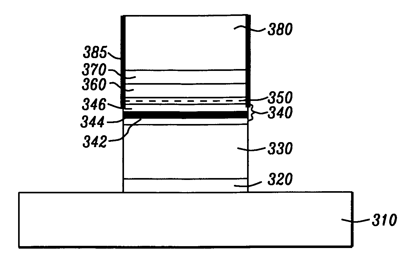
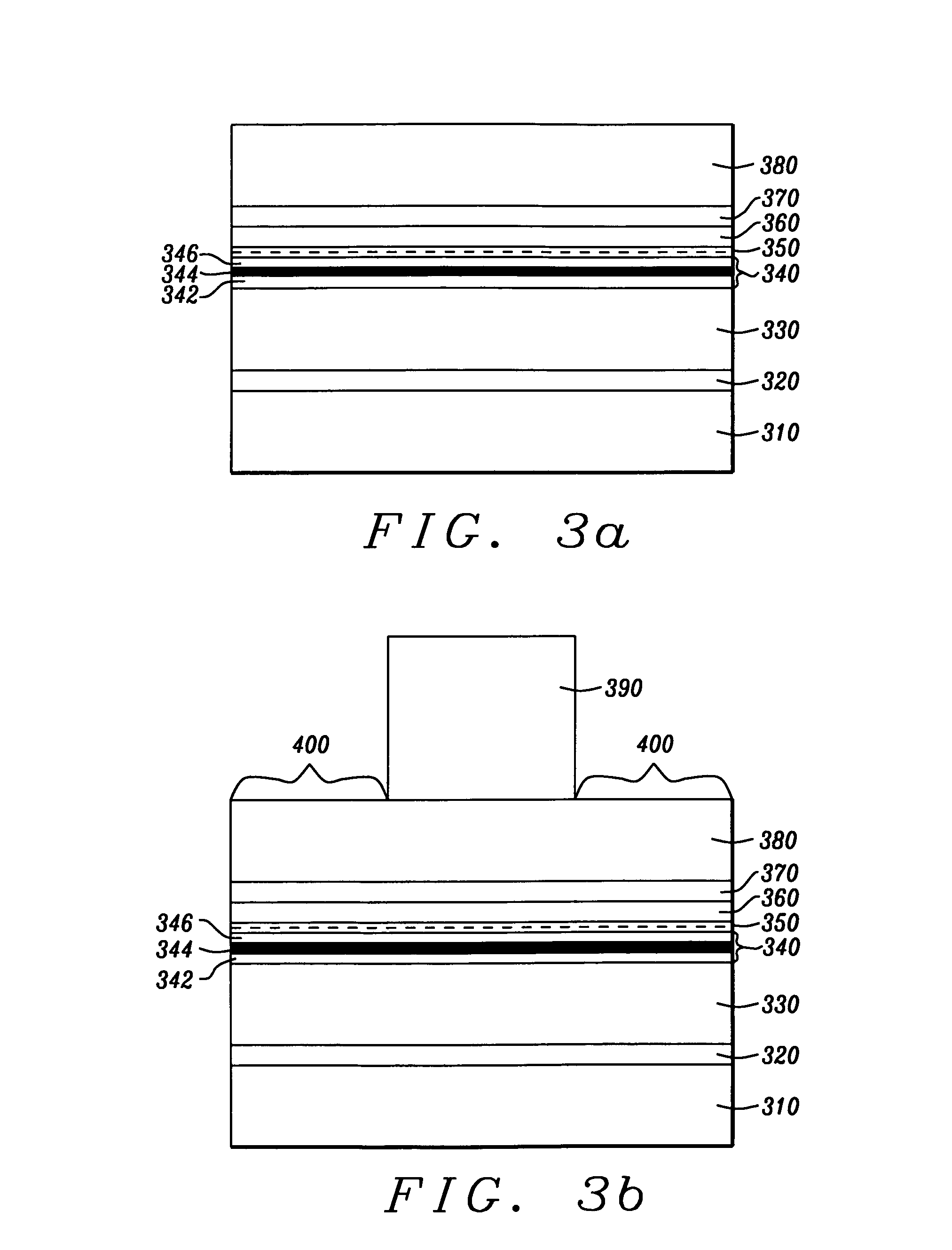
[0043]The preferred embodiment of the present invention is the formation of a patterned MTJ stack using a reactive ion etch (RIE) and the production, thereby, of an MTJ cell that is free of electrical shorting and suitable for use in an MRAM array.

[0044]Referring to FIG. 3a, there is shown a schematic vertical cross-sectional view of a horizontally multi-layered MTJ stack of a material structure, dimensions and configuration to be effectively patterned by the method of the present invention. The lower layer (310) is a bottom electrode for the purpose of injecting a current. On this electrode will be formed a horizontally multi-layered magnetically pinned structure that comprises a seed layer (320) of NiCr formed to a thickness between approximately 30 and 60 Angstroms, an antiferromagnetic layer (330), typically of MnPt formed to a thickness between approximately 120 and 300 Angstroms, but which can be IrMn, MnNi or any intrinsic antiferromagnetic material that can exchange couple w...


PUM


Abstract

An MTJ cell without footings and free from electrical short-circuits across a tunneling barrier layer is formed by using a Ta hard mask layer and a combination of etches. A first etch patterns the Ta hard mask, while a second etch uses O2 applied in a single high power process at two successive different power levels. A first power level of between approximately 200 W and 500 W removes BARC, photoresist and Ta residue from the first etch, the second power level, between approximately 400 W and 600 W continues an etch of the stack layers and forms a protective oxide around the etched sides of the stack. Finally, an etch using a carbon, hydrogen and oxygen gas completes the etch while the oxide layer protects the cell from short-circuits across the lateral edges of the barrier layer.

Description

BACKGROUND OF THE INVENTION[0001]1. Field of the Invention[0002]This invention relates to the fabrication of a magnetic random access memory (MRAM) device using a magnetic tunneling junction (MTJ) cell and more particularly to a method of its fabrication that results in the elimination of electrical shorting.[0003]2. Description of the Related Art[0004]The magnetic tunneling junction (MTJ) device, is a form of tunneling magnetoresistive (TMR) device in which the relative orientation of uni-directional magnetic moments in parallel, vertically separated upper and lower magnetized layers, controls the flow of spin-polarized electrons tunneling through a very thin dielectric layer (the tunneling barrier layer) formed between those layers. When injected electrons pass through the upper layer they are spin polarized by interaction with the magnetic moment of that layer. The probability of such an electron then tunneling through the intervening tunneling barrier layer into the lower layer ...

Claims


Application Information

Patent Timeline
Patent Type & Authority Patents(United States)
IPC IPC(8): G11C11/02
CPCH01L43/12H01L43/08H10N50/10H10N50/01
Inventor XIAO, RONGFUTORNG, CHYU-JIUHZHONG, TOMKULA, WITOLD
Owner TAIWAN SEMICON MFG CO LTD
Why Eureka
Try Eureka