Memory control circuit and memory accessing method

a memory control circuit and memory accessing technology, applied in the field of memory control circuits, can solve the problems of time-consuming, challenging, and difficult to design the corresponding logic for all those logics, and achieve the effect of simplifying and unifying the erase operation

Inactive Publication Date: 2011-05-03
MACRONIX INT CO LTD
View PDF4 Cites 11 Cited by
  • Summary
  • Abstract
  • Description
  • Claims
  • Application Information

AI Technical Summary

Benefits of technology

[0013]The invention is directed to a memory control circuit for performing erase verification on a memory circuit including lots of memory blocks. The memory control circuit can effectively simplify and unify the erase operation on the boundary of different memory blocks.

Problems solved by technology

Thus, additional logic circuits and control signals are needed to control the operation of the bias circuit BS2 based on the two sensed result is a challenging task.
Thus, it is challenging and time-consuming to design corresponding logic for all those logic control.

Method used


Image

  • Memory control circuit and memory accessing method
  • Memory control circuit and memory accessing method
  • Memory control circuit and memory accessing method

Examples


Embodiment Construction

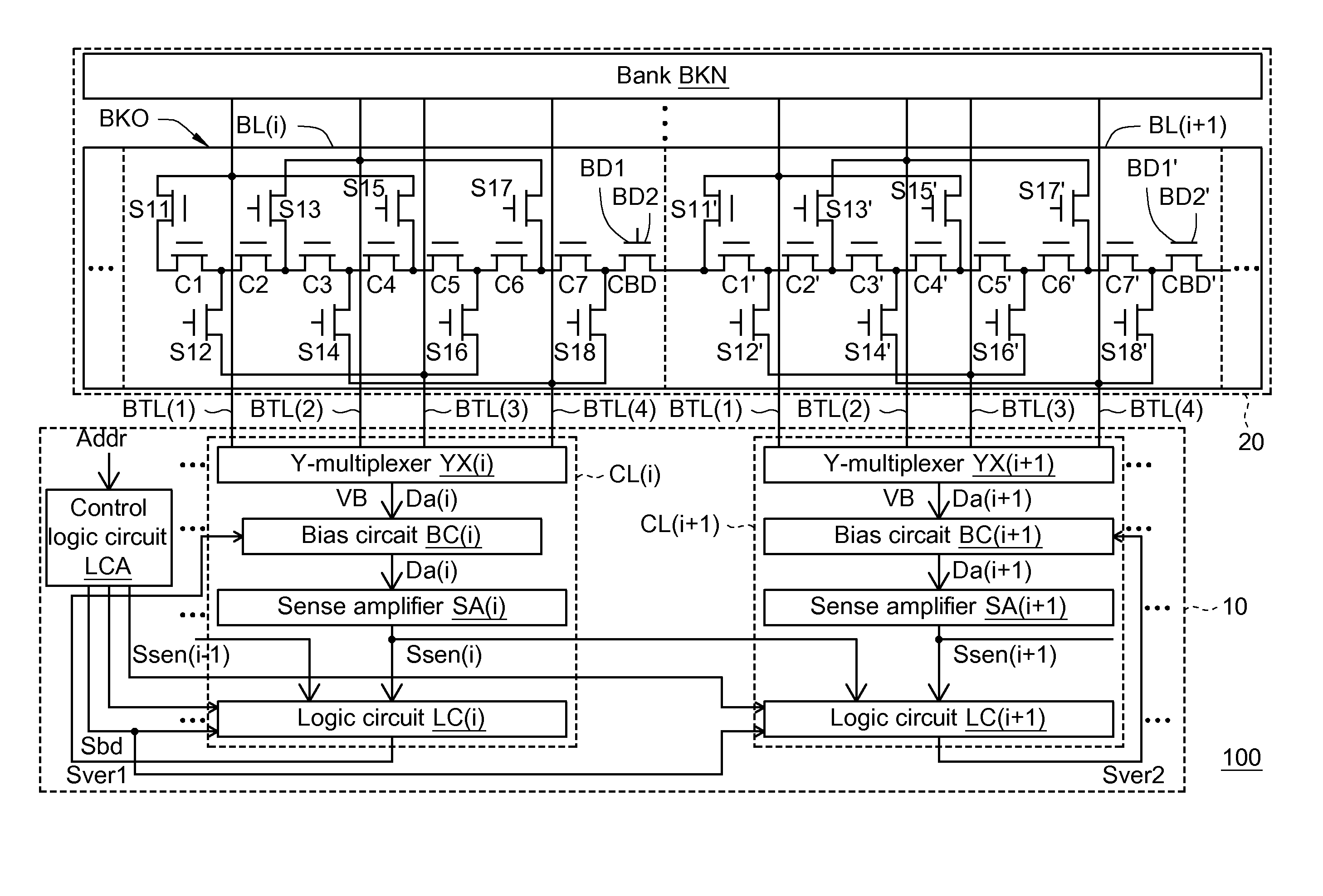
[0022]According to an embodiment of invention, a memory control circuit is provided to read the boundary data of the boundary cells of the corresponding memory blocks in response to one column selection signal. Thus, the operations of the logic circuits in each control units, which correspond with the respective memory blocks, can be simplified and unified.

[0023]Generally, in an erase verification operation performed on a particular memory block, data stored in the memory cells of the memory block are read and used to determine whether the corresponding memory cells are erased. For example, when the data has a value of 1, it is suggested that the corresponding memory cell is erased. When the data a value of 0, it is suggested that the corresponding memory cell is not erased. In the following passages, an example for an erase operation and an erase verification operation performed on a memory will be provided for detailed explanation.

[0024]Referring to FIG. 3, a block diagram of a me...


PUM


Abstract

A control circuit applied in a memory that comprises a first memory block and a second memory block, and each of the first and the second memory blocks includes a boundary cell. The control circuit comprises an address decoder, a first Y-multiplexer, and a second Y-multiplexer. The address decoder provides a plurality of column selection signals capable of being a boundary value. The first Y-multiplexer corresponds to the first memory block and provides a first boundary data channel for a boundary cell of the first memory block. The second Y-multiplexer corresponds to the second memory block and provides a second boundary data channel for a boundary cell of the second memory block. The first and the second boundary data channels are enabled simultaneously in response to the boundary value for outputting boundary data stored in the boundary cell of the first memory block and that of the second memory block.

Description

[0001]This application claims the benefit of U.S. application Ser. No. 61 / 048,247, filed Apr. 28, 2008, the subject matter of which is incorporated herein by reference.BACKGROUND OF THE INVENTION[0002]1. Field of the Invention[0003]The invention relates in general to a memory control circuit, and more particularly to a memory control circuit performing erase verification operation on a memory array of a memory.[0004]2. Description of the Related Art[0005]Referring to FIG. 1, a schematic illustration of a conventional memory is shown. In an example, a memory array MA includes memory banks BNK0 to BNKN, each of which includes M memory blocks, wherein N is a natural number greater than 1 and M is a natural number greater than 1. For example, the memory bank BNK0 includes memory blocks BLO1 to BLOM. Since an erase process and an erase verification process performed on each of the memory blocks BLO1 to BLOM are similar, only the process performed on the memory block BLO1 is cited as an e...

Claims


Application Information

Patent Timeline
Patent Type & Authority Patents(United States)
IPC IPC(8): G11C8/00
CPCG11C7/1006G11C8/12G11C7/1012G11C2207/005G11C2207/002
Inventor CHEN, CHUNG-KUANGSHIH, YI-TEHUNG, CHUN-HSIUNG
Owner MACRONIX INT CO LTD
Why Eureka
Try Eureka