Array of processing elements with local registers

a processing element and register technology, applied in image memory management, single instruction multiple data multiprocessors, instruments, etc., can solve the problems of limiting the maximum operating frequency, affecting the speed of copy operation, and disadvantageous for higher operating frequencies, so as to slow down the loading of pixels

Inactive Publication Date: 2011-05-10
INTERDIGITAL VC HLDG INC
View PDF19 Cites 90 Cited by
  • Summary
  • Abstract
  • Description
  • Claims
  • Application Information

AI Technical Summary

Benefits of technology

[0016]Further, in one embodiment of the invention, the memory subsystem of each PE contains extension areas that serve as reference pixel load areas, i.e. storage areas for pixels that are not in the current run compared to the current pixel, but in the next run. This allows relatively slow loading of pixels from the main image memory, since writing to the extension areas and processing / shifting the main search area of the memory does not interfere. The main search area can be shifted separately in such mode. Due to this loading capability it is possible to extend the reference blocks in an arbitrary way, simultaneously to processing the other data.

Problems solved by technology

This copy operation takes relatively long, since the large image memory is slow.
Crossbar switches commonly contain a high number of multiplexer elements in a deep hierarchy, which is disadvantageous for higher operating frequencies.
However, known implementations generally suffer from the long and complicated connection paths between the PE and the memory subsystem, and the resulting limitation of maximum operating frequency.

Method used


Image

  • Array of processing elements with local registers
  • Array of processing elements with local registers
  • Array of processing elements with local registers

Examples


Embodiment Construction

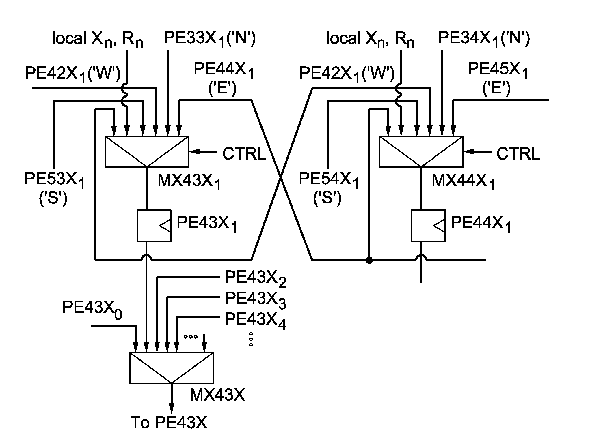
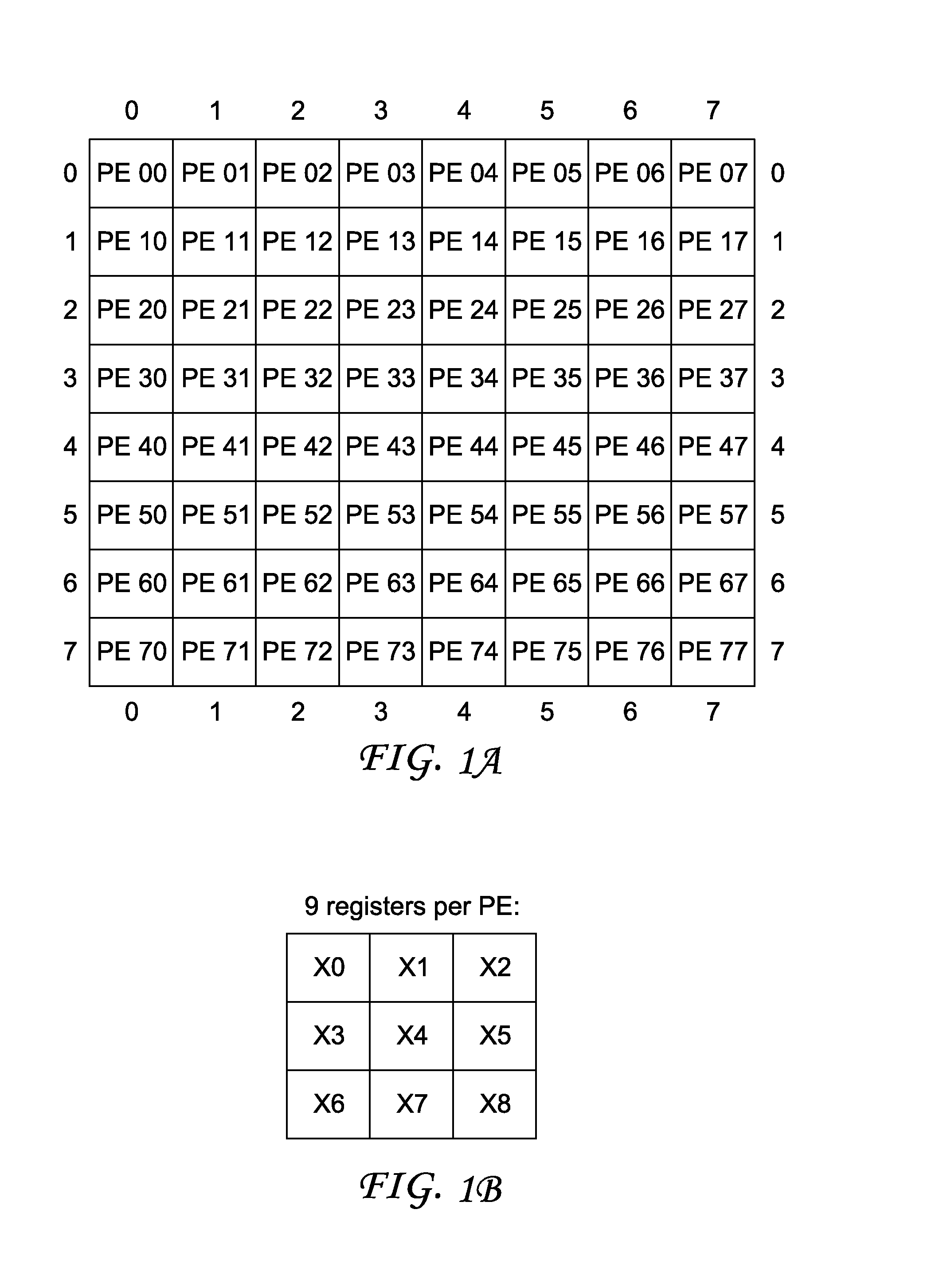
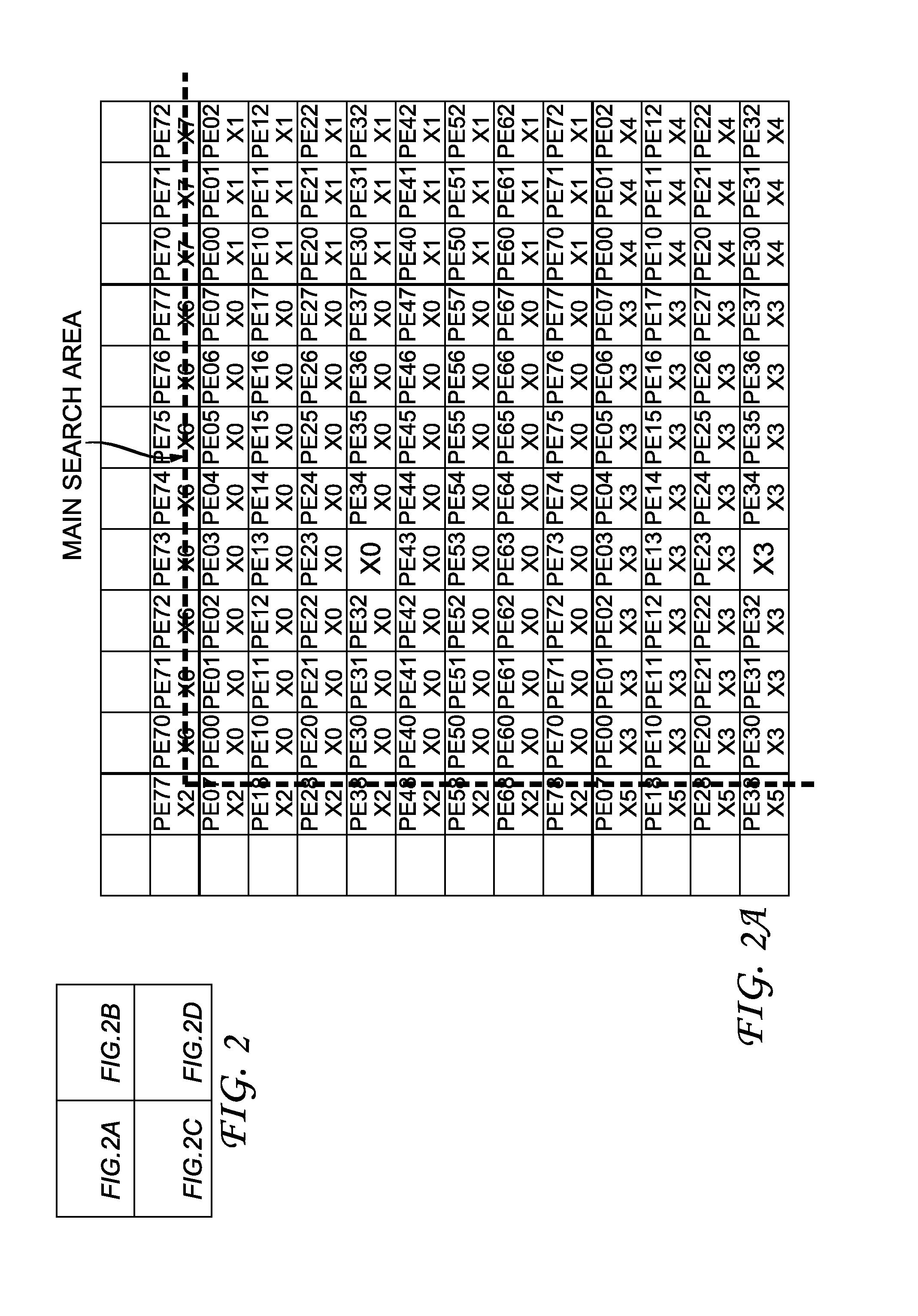
[0025]For motion estimation, a best match position for a given block in a previous field / frame is searched. To achieve this, a given block has to be compared to many positions in a search area. To achieve the necessary processing speed, a parallel hardware with one PE per pixel is used. This may be implemented as a two-dimensional array or grid of PEs, as shown in FIG. 1. In this embodiment of the invention, each PE has nine special registers X0, . . . , X8, each of which holding a reference pixel value. E.g. one register X0 holds the corresponding pixel of the corresponding block of the reference image, three registers X1, X3, X4 hold corresponding pixels of neighboring blocks of the reference image that may be used for larger block sizes like 8×16, 16×8, 16×16, and five registers X2, X5, X6, X7, X8 are used to buffer pixels that are shifted in or out the 16×16 block X0-X1-X3-X4 as described below. The neighboring reference blocks are e.g. those that are referred to as east X1, sou...


PUM


Abstract

Specialized image processing circuitry is usually implemented in hardware in a massively parallel way as a single instruction multiple data (SIMD) architecture. The invention prevents long and complicated connection paths between a processing element and the memory subsystem, and improves maximum operating frequency. An optimized architecture for image processing has processing elements that are arranged in a two-dimensional structure, and each processing element has a local storage containing a plurality of reference pixels that are not neighbors in the reference image. Instead, the reference pixels belong to different blocks of the reference image, which may vary for different encoding schemes. Each processing element has a plurality of local first registers for holding the reference image data: one of the first registers holds reference input data of a first search block, and some of the remaining first registers holding reference input data of further search blocks that have specified positions relative to the first search block.

Description

[0001]This application claims the benefit, under 35 U.S.C. §119 of EP Patent Application 06301200.9, filed 1 Dec. 2006.FIELD OF THE INVENTION[0002]This invention relates to an array of processing elements having local registers for input data.BACKGROUND[0003]Motion estimation (ME) is an example for a time critical application that requires very much processing power. Therefore, specialized circuitry is usually implemented in hardware in a massively parallel way as single instruction multiple data (SIMD) architectures. These architectures have commonly one processing element (PE) per value to be calculated, e.g. for comparing a pixel of a current picture to reference pixels. Usually, the corresponding pixel in the previous picture and its neighbors serve as reference pixel. In a more generalized view, any one-, two- or multi-dimensional data set serves as input to the processing. The PE for ME can access a current pixel and a number of reference pixels stored in a memory. The pixels ...

Claims


Application Information

Patent Timeline
Patent Type & Authority Patents(United States)
IPC IPC(8): G06F15/00
CPCG06T1/60G06F15/8023
Inventor GEORGI, MARCOGAEDKE, KLAUSBORSUM, MALTE
Owner INTERDIGITAL VC HLDG INC
Why Eureka
Try Eureka