Manufacturing method of light-emitting device

a manufacturing method and technology of light-emitting devices, applied in the field of fabrication systems, can solve the problems of extremely low efficiency of utilizing expensive el materials, high manufacturing cost of light-emitting devices, and 1% or less, and achieve the effects of reducing heating time, increasing vacuum, and uniform film thickness

Inactive Publication Date: 2011-05-17
SEMICON ENERGY LAB CO LTD
View PDF199 Cites 15 Cited by
  • Summary
  • Abstract
  • Description
  • Claims
  • Application Information

AI Technical Summary

Benefits of technology

[0012]Hence, the present invention provides a vapor deposition system of fabrication systems that promotes an efficiency of utilizing an EL material to reduce manufacturing costs and is excellent in uniformity or throughput of forming an EL layer and a vapor deposition method. Further, the present invention provides a light emitting apparatus fabricated by the vapor deposition system and the vapor deposition method according to the present invention and a manufacturing method of the light emitting apparatus.
[0013]Further, the invention provides a fabrication system for vapor-depositing an EL material efficiently on a large area substrate having a size of, for example, 320 mm×400 mm, 370 mm×470 mm, 550 mm×650 mm, 600 mm×720 mm, 680 mm×880 mm, 1000 mm×1200 mm, 1100 mm×1250 mm or 1150 mm×1300 mm. Also, the present invention provides a vapor deposition system that makes a whole surface of a large area substrate uniform with even thickness.

Problems solved by technology

Therefore, in forming the EL layer, an efficiency of utilizing the expensive EL materials is extremely low i.e. about 1% or less and manufacturing cost of a light emitting apparatus becomes very high.
Also, in using a large area substrate, it may be a problem that the film thickness between a center portion and a marginal portion of a substrate is uneven.
Further, the vapor deposition system has a structure for rotating a substrate and therefore, there is a limit in the vapor deposition system aiming at a large area substrate.

Method used


Image

  • Manufacturing method of light-emitting device
  • Manufacturing method of light-emitting device
  • Manufacturing method of light-emitting device

Examples


embodiment mode 1

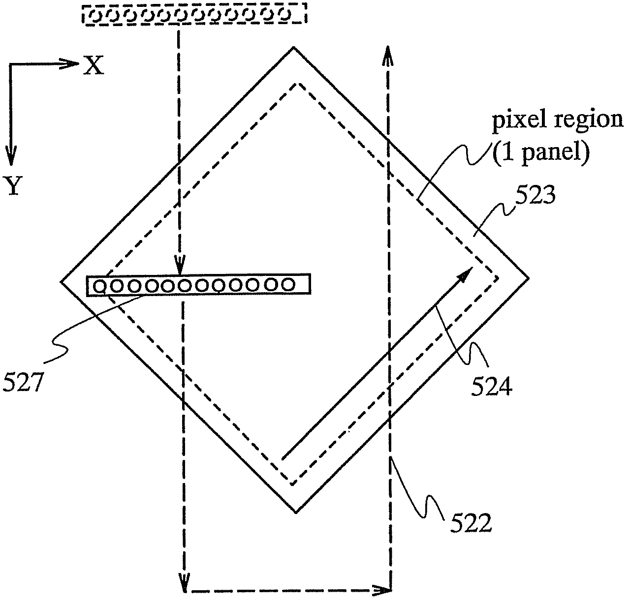
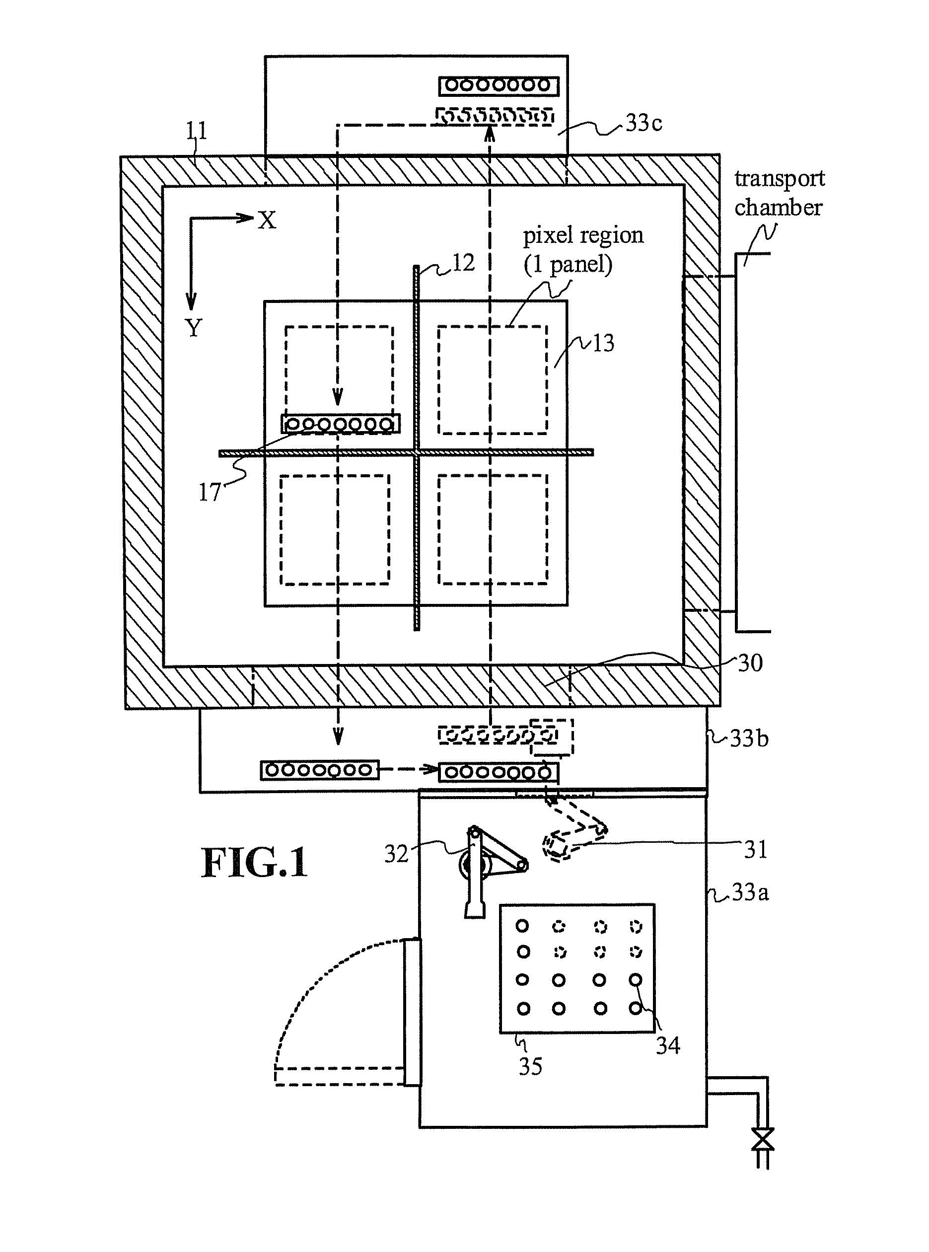
[0111]FIG. 1 is a top view showing a vapor deposition system according to the present invention. FIG. 1 shows the vapor deposition system in the midst of vapor deposition.

[0112]In FIG. 1, a film formation chamber 11 includes a substrate holding means 12, an evaporation source holder 17 installed with an evaporation shutter, a mechanism for moving the evaporation source holder (not shown), and means for producing a low pressure atmosphere (vacuum exhausting means). Further, a large-size substrate 13 and a deposition mask 14(not shown) are installed in the film formation chamber 11.

[0113]Further, the substrate holding means 12 fixes by gravitation the deposition mask 14 made of a metal and therefore fixes the substrate 13 which is arranged over the deposition mask. Note that the substrate holding means 12 may be installed for a vacuum suction mechanism to fix the mask. An example of adhesion or welding of the deposition mask to the substrate holding means 12 is shown here. However, in...

embodiment mode 2

[0137]Next, a detailed description will be given of a structure of a substrate holding means according to the invention in reference to FIGS. 3A to 3H.

[0138]FIG. 3A shows a perspective view of a substrate holding means 301 mounted with a substrate 303 and a mask 302 and FIG. 3B shows only the substrate holding means 301.

[0139]Further, FIG. 3C shows a cross sectional view of the substrate holding means mounted with the substrate 303 and the mask 302 which is constituted by a metal plate (representatively, Ti) having a height h of 10 mm through 50 mm and a width w of 1 mm through 5 mm.

[0140]By the substrate holding means 301, bending of the substrate or bending of the mask can be restrained.

[0141]Further, the shape of the substrate holding means 301 is not limited to that shown by FIGS. 3A through 3C but may be constituted by a shape as shown in, for example, 3E.

[0142]FIG. 3E shows an example of providing portions that support end portions of the substrate and by a substrate holding m...

embodiment mode 3

[0146]An example of the film formation chamber having multiple evaporation source holders is given in Embodiment Mode 1. In the other hand, in Embodiment Mode 3, an example of a film formation chamber having one evaporation source holder in FIGS. 4A-B.

[0147]FIGS. 4A and 4B show a vapor deposition system according to the present invention. FIG. 4A is a cross sectional view in a Y-direction (taken along a dotted line A-A′) and FIG. 4B is a top view. FIGS. 4A and 4B show the vapor deposition system in the midst of vapor deposition.

[0148]In FIG. 4A, a film formation chamber 411 has a substrate holding means 412, an evaporation source holder 417 provided with an evaporation shutter, a moving mechanism 420 for moving the evaporation source holder, and a means for producing the low pressure atmosphere. A large-sized substrate 413 and a deposition mask 414 are also installed in the film formation chamber 411. In addition, the deposition mask 414 made of metal is fixed in the substrate holdi...


PUM

PropertyMeasurementUnit
angleaaaaaaaaaa
angleaaaaaaaaaa
distanceaaaaaaaaaa

Abstract

The present invention provides a vapor deposition method and a vapor deposition system of film formation systems by which EL materials can be used more efficiently and EL materials having superior uniformity with high throughput rate are formed. According to the present invention, inside a film formation chamber, an evaporation source holder in a rectangular shape in which a plurality of containers sealing evaporation material is moved at a certain pitch to a substrate and the evaporation material is vapor deposited on the substrate. Further, a longitudinal direction of an evaporation source holder in a rectangular shape may be oblique to one side of a substrate, while the evaporation source holder is being moved. Furthermore, it is preferable that a movement direction of an evaporation source holder during vapor deposition be different from a scanning direction of a laser beam while a TFT is formed.

Description

[0001]This application is a divisional of U.S. application Ser. No. 10 / 664,642, filed on Sep. 19, 2003 now abandoned.BACKGROUND OF THE INVENTION[0002]1. Field of the Invention[0003]The present invention relates to a fabrication system having a film formation system for depositing materials which can be deposited by vapor deposition (hereinafter, an evaporation material), a light emitting device which has a film containing an organic compound as a light emitting layer and for which the fabrication system is used, and a manufacturing method thereof. Specifically, the present invention relates to a film formation method (a vapor deposition method) for forming a film by vaporizing an evaporation material from a plurality of evaporation sources provided to be opposite to a substrate and a fabrication system.[0004]2. Description of the Related Art[0005]In recent years, research related to a light emitting apparatus having an EL device as a self-luminous light emitting device has been acti...

Claims


Application Information

Patent Timeline
Patent Type & Authority Patents(United States)
IPC IPC(8): H01L21/84C23C14/04C23C14/12C23C14/24C23C14/50C23C14/56H01L27/32H01L51/56H05B33/10H05B33/14
CPCC23C14/046C23C14/12C23C14/246H01L33/44H01L51/56C23C14/564H01L27/3244H10K59/12H10K71/00H05B33/10H01L21/00C23C16/00H01L21/18
Inventor YAMAZAKI, SHUNPEIKUWABARA, HIDEAKIMURAKAMI, MASAKAZU
Owner SEMICON ENERGY LAB CO LTD
Why Eureka
Try Eureka