
Eureka
For R&D, Eureka makes reading and utilizing patents & technical documents easy.
Eureka AIR
Designed for self-driven R&D workflows. Generate viable solutions, solve complex R&D challenges, empower your innovation with AI.

Eureka Materials
Designed for material experts only. Revolutionize your material R&D, from search, analyze, to developing new materials.

TechResearch
Generate reliable direction feasibility study reports for your R&D in just a few steps.

TechSeek
Discover and master advanced knowledge NOW. Basics, ideas, possibilities, all at once.

TechMind
As an expert in R&D Theories, TechMind can generates customized viable solutions instantly.

TechRisk
Analyze your overall solution with one click, know your potential R&D risks in advance.

TechMonitor
Get weekly tech updates, stay abreast of the latest tech innovations and key insights.
Method for forming electrode for group-III nitride compound semiconductor light-emitting devices
a technology of nitride and compound semiconductors, which is applied in the direction of semiconductor lasers, semiconductor devices, semiconductor devices, etc., can solve the problems of low light extraction efficiency of conventional group-iii nitride compound semiconductor light-emitting devices, and the bonding strength between aluminum and gallium nitride or the like is not necessarily high, and achieves high reflectivity
- Summary
- Abstract
- Description
- Claims
- Application Information
AI Technical Summary
Benefits of technology
Problems solved by technology
Method used
Image

Examples
example 1
[0041]Electrodes according to the present invention were measured for contact resistance with respect to n-type GaN as described below.
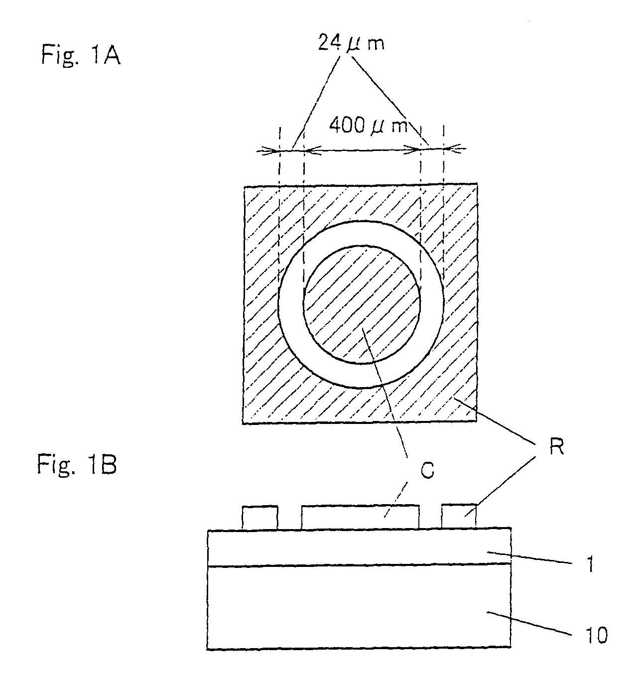
[0042]FIG. 1A is a plan view of a structure including a first electrode C and second electrode R measured for contact resistance. FIG. 1B is a sectional view of the structure. As shown in FIG. 1B, a buffer layer (not shown) made of aluminum nitride (AlN) was formed on a sapphire substrate 10. A layer of GaN was formed on the buffer layer by MOVPE so as to have a thickness of about 4 μm and then doped with Si at a dose of 4×1018 cm−3, whereby an n-type GaN layer 1 was formed. The first and second electrodes C and R were formed on the n-type GaN layer 1 by vacuum vapor deposition. The first and second electrodes C and R may be formed by a sputtering process.
[0043]As shown in FIG. 1A, the first electrode C was disk-shaped and had a diameter of 400 μm. The second electrode R was spaced from the first electrode C at a distance of 24 μm and was ring-shaped...
example 2
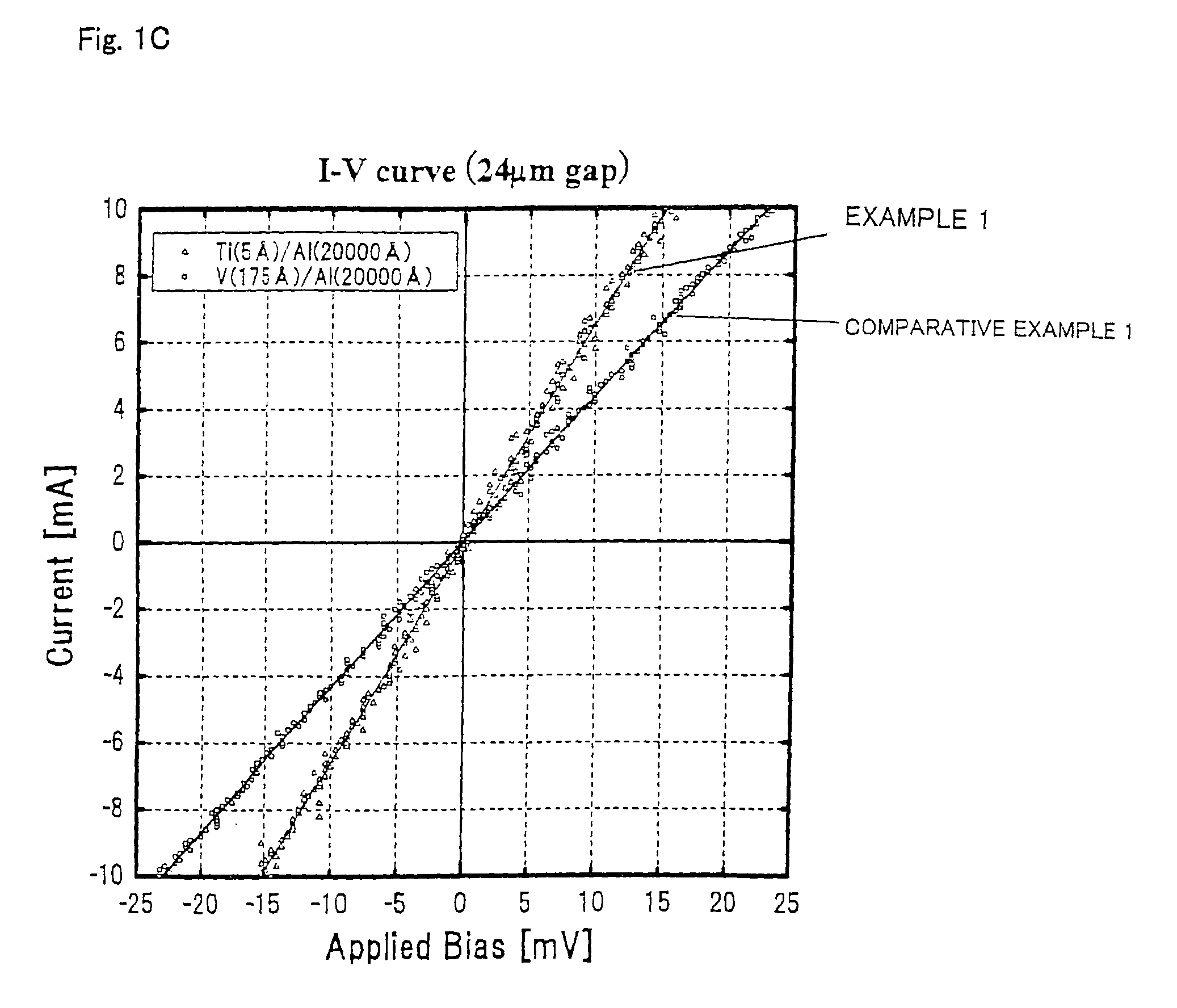
[0048]An electrode according to the present invention was evaluated for reflectivity by a method below.
[0049]A first sample including a first sapphire substrate with a thickness of 400 μm and a first electrode disposed thereon was prepared in such a manner that a titanium (Ti) layer with a thickness of 0.5 nm (5 Å) and a first aluminum (Al) layer with a thickness of 2 μm were deposited on the first sapphire substrate in that order (Example 2).
[0050]A second sample, including a second sapphire substrate with a thickness of 400 μm and a second electrode disposed thereon, for comparison was prepared in such a manner that a first vanadium (V) layer with a thickness of 17.5 nm (175 Å) and a second aluminum (Al) layer with a thickness of 2 μm were deposited on the second sapphire substrate in that order (Comparative Example 2).
[0051]A third sample, including a third sapphire substrate and a third electrode disposed thereon, for comparison was prepared in such a manner that a third aluminu...
example 3
[0063]Light-emitting devices were prepared and then evaluated as described below.
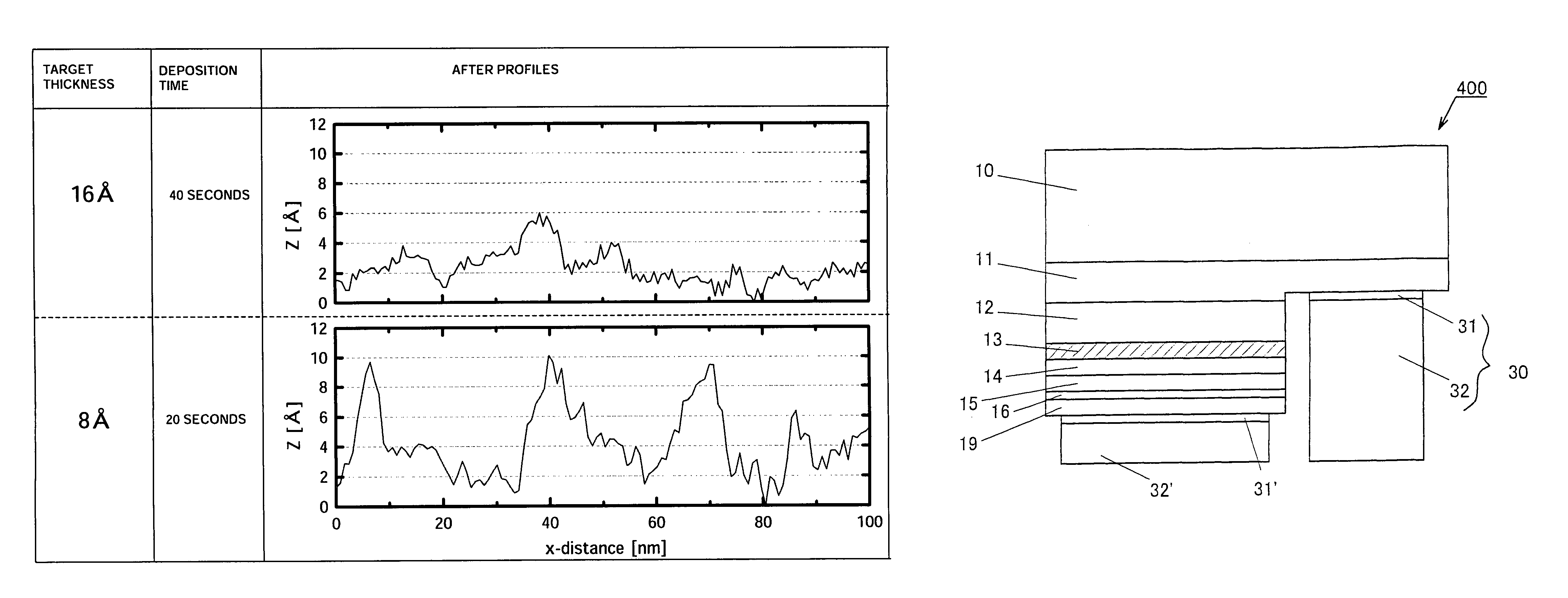
[0064]FIG. 3 is a sectional view of a first Group-III nitride compound semiconductor light-emitting device 100 according to an embodiment of the present invention. The first Group-III nitride compound semiconductor light-emitting device 100 includes a sapphire substrate 10, a buffer layer (not shown) made of aluminum nitride (AlN), an n-type GaN layer 11 doped with Si, an n-type AlGaN clad layer 12 doped with Si, a light-emitting layer 13 having a GaN / InGaN multi-quantum well structure, a p-type AlGaN clad layer 14 doped with Mg, a p-type GaN layer 15 doped with Mg, and a p+-type GaN layer 16, these layers being deposited on the sapphire substrate 10 by MOCVD or MOPVD in that order.
[0065]The first Group-III nitride compound semiconductor light-emitting device 100 further includes a translucent electrode 21, made of ITO, extending over the p+-type GaN layer 16; a pad electrode 22, made of gold, lying on ...
PUM
| Property | Measurement | Unit |
|---|---|---|
| thickness | aaaaa | aaaaa |
| thickness | aaaaa | aaaaa |
| reflectivity | aaaaa | aaaaa |
Abstract
Description
Claims
Application Information
 - R&D Engineer
- R&D Manager
- IP Professional
- Industry Leading Data Capabilities
- Powerful AI technology
- Patent DNA Extraction
Browse by: Latest US Patents, China's latest patents, Technical Efficacy Thesaurus, Application Domain, Technology Topic, Popular Technical Reports.
© 2024 PatSnap. All rights reserved.Legal|Privacy policy|Modern Slavery Act Transparency Statement|Sitemap|About US| Contact US: help@patsnap.com