Semiconductor integrated circuit device and countermeasure method against NBTI degradation

a technology of integrated circuits and semiconductors, applied in the direction of generating/distributing signals, pulse techniques, instruments, etc., can solve problems such as performance degradation, erroneous operation, and margin generation

Active Publication Date: 2011-05-24
KK TOSHIBA
View PDF5 Cites 12 Cited by
  • Summary
  • Abstract
  • Description
  • Claims
  • Application Information

AI Technical Summary

Problems solved by technology

When the threshold voltage shifts to the negative side, a drive current (drain current) at the time of an operation of the PMOS transistor used by flowing current decreases, thereby causing a problem of performance degradation.
Further, when NBTI degradation occurs in a clock path, an erroneous operation due to clock skew occurs because a delay variation amount due to the degradation is different in each path.
However, in a designing method taking the time margin after NBTI degradation into consideration, an over margin is generated.
This causes problems such that a circuit size increases to incur cost increase, circuit characteristics deteriorate due to interruption of a high-speed operation, and further cost increase is incurred due to a prolonged development period.
However, these patent applications only disclose a technique for preventing the occurrence of erroneous operations due to clock skew mentioned above, and do not disclose measures against performance degradation due to NBTI degradation in a data path in a flip-flop circuit.

Method used


Image

  • Semiconductor integrated circuit device and countermeasure method against NBTI degradation
  • Semiconductor integrated circuit device and countermeasure method against NBTI degradation
  • Semiconductor integrated circuit device and countermeasure method against NBTI degradation

Examples


first embodiment

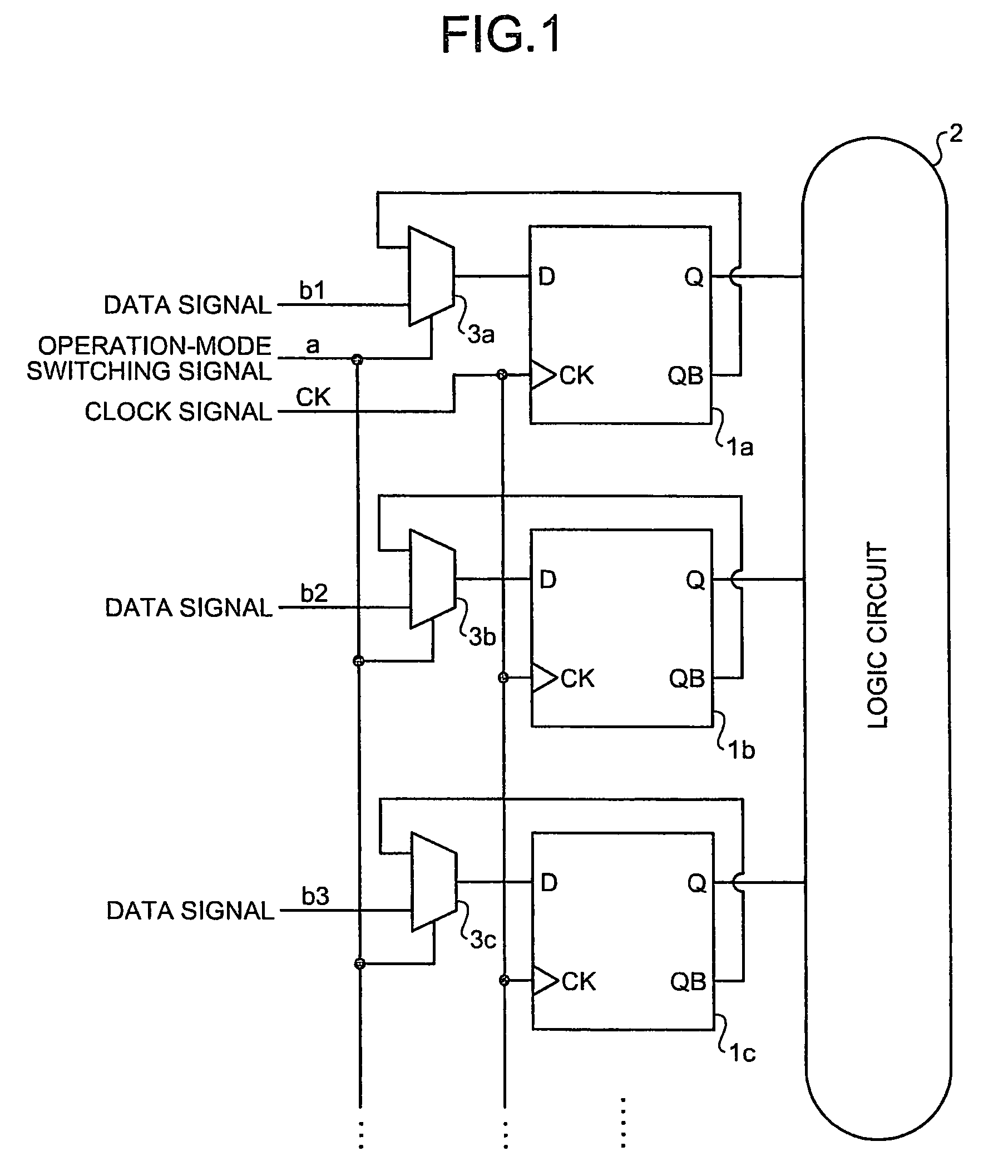
[0020]FIG. 1 is a block diagram of a configuration of relevant parts of a semiconductor integrated circuit device according to the present invention. In FIG. 1, in the semiconductor integrated circuit device, as at least one flip-flop circuit (hereinafter, “FF circuit”), which is a target circuit of the low power consumption mode, and a logic circuit to which each output of the at least one FF circuit is input, for example, FF circuits 1a, 1b, and 1c, and a logic circuit 2 to which respective data outputs (Q output) of the FF circuits 1a, 1b, and 1c are shown.

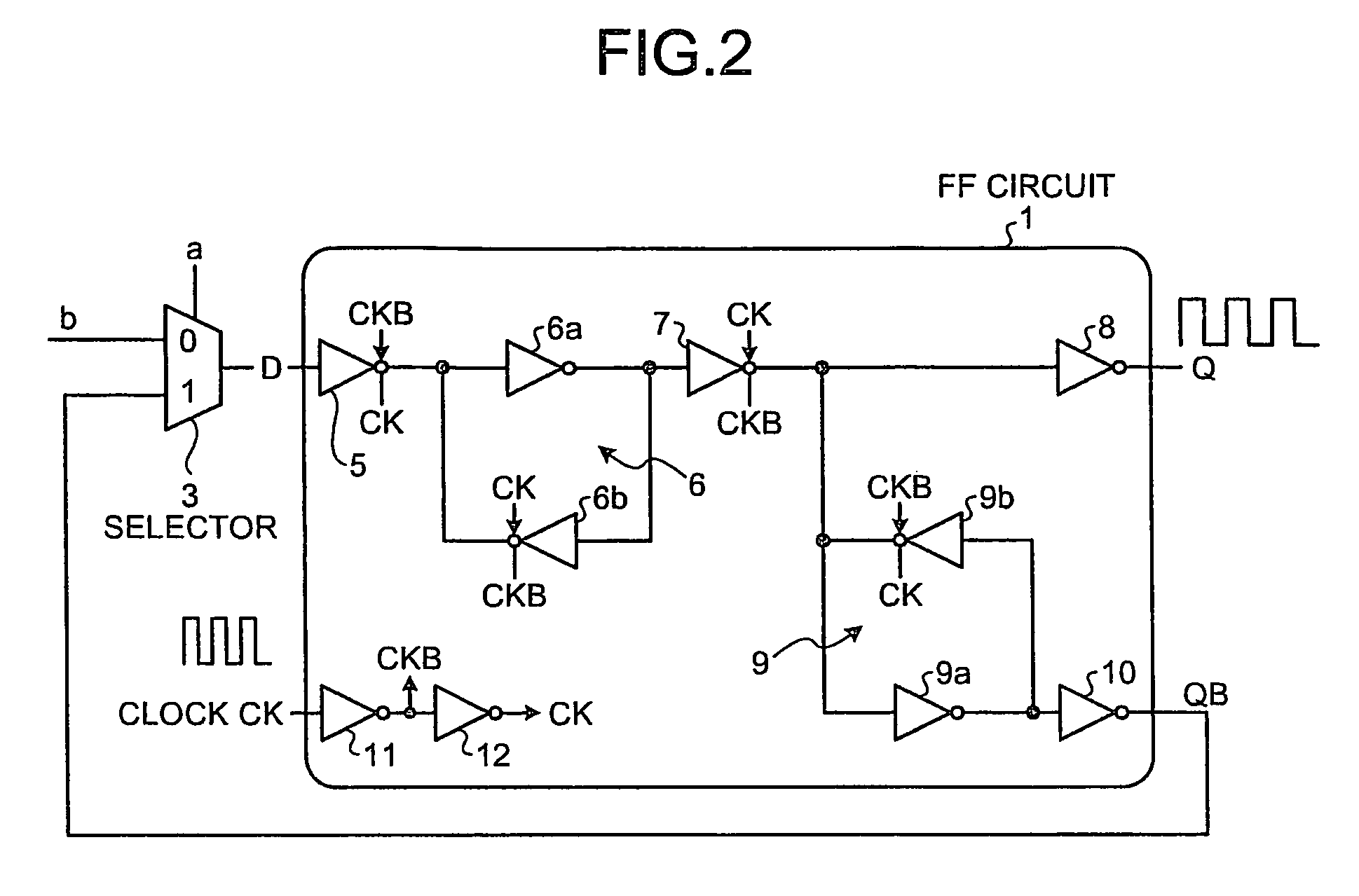
[0021]As shown in FIG. 1, selectors 3a, 3b, and 3c are provided on a side of data input terminals D of respective FF circuits 1a, 1b, and 1c. As an arrangement relationship of the selectors 3 (3a, 3b, and 3c) with respect to the FF circuits 1 (1a, 1b, and 1c), the arrangement relationship is shown by dividing it by functions in FIG. 1 and other drawings. However, as the actual arrangement relationship, needless to say, there ar...

second embodiment

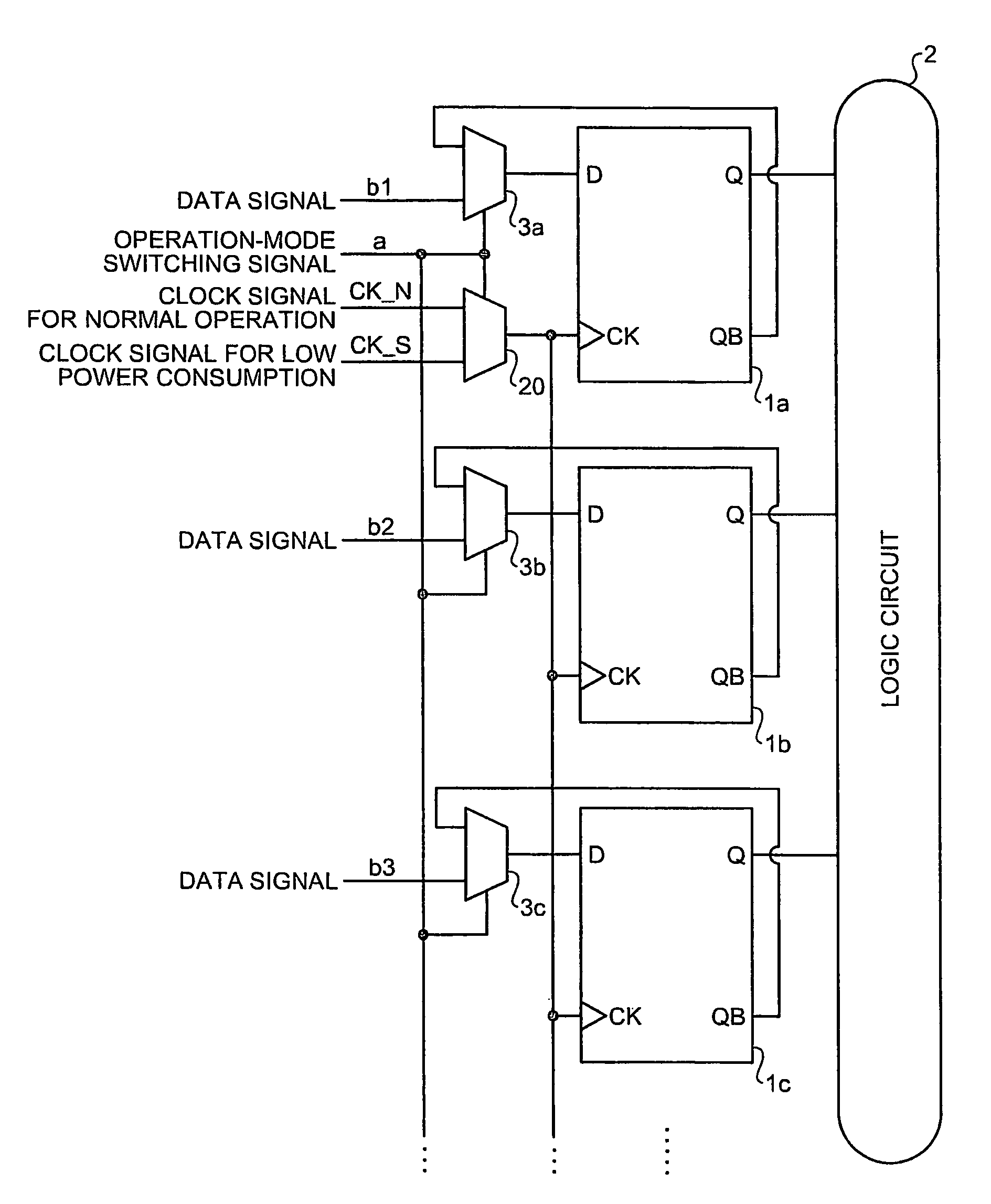
[0035]As shown in FIG. 3, in the semiconductor integrated circuit device a selector 20, which is a clock selector, is added in the configuration shown in FIG. 1 (the first embodiment).

[0036]A clock signal CK_N for a normal operation and a clock signal CK_S for low power consumption are input to the selector 20. The output terminal of the selector 20 is commonly connected to the clock input terminal CK of the FF circuits 1a, 1b, and 1c. A switching control signal to the selector 20 is the operation-mode switching signal “a” same as in the case of the selector 3.

[0037]In the example shown in FIG. 3, the selector 20 selects the clock signal CK_N for a normal operation and transmits the signal to the clock input terminal CK when the operation-mode switching signal “a” is at the low level “0”, or selects the clock signal CK_S for low power consumption and transmits the signal to the clock input terminal CK when the operation-mode switching signal “a” is at the high level “1”.

[0038]The c...


PUM


Abstract

A semiconductor integrated circuit device includes a target circuit of a low power consumption mode having at least one flip-flop circuit to which a clock signal is supplied in a normal operation mode and in a low power consumption mode, and a logic circuit to which each output of the at least one flip-flop circuit is input, wherein each of the flip-flop circuits includes a selector that selects a normal data signal in the normal operation mode, selects an inverted output of the flip-flop circuit in the low power consumption mode, based on an operation-mode switching signal that designates switching between the normal operation mode and the low power consumption mode, and inputs the selected signal to a data input terminal of the flip-flop circuit.

Description

CROSS-REFERENCE TO RELATED APPLICATIONS[0001]This application is based upon and claims the benefit of priority from the prior Japanese Patent Application No. 2008-150861, filed on Jun. 9, 2008; the entire contents of which are incorporated herein by reference.BACKGROUND OF THE INVENTION[0002]1. Field of the Invention[0003]The present invention relates to a semiconductor integrated circuit device and a countermeasure method against NBTI degradation.[0004]2. Description of the Related Art[0005]In a flip-flop circuit included in a semiconductor integrated circuit device, when a high-level or low-level fixed value is input in a low power consumption mode, there is a part in a circuit where a fixed-value negative bias voltage is applied to a gate electrode of a P-channel metal oxide semiconductor (PMOS) transistor. In such a PMOS transistor applied with the fixed-value negative bias voltage, electric current does not flow and the PMOS transistor becomes an ON state. When this situation i...

Claims


Application Information

Patent Timeline
Patent Type & Authority Patents(United States)
IPC IPC(8): H03K19/003
CPCH03K19/00369
Inventor KAWAKAMI, SHINYA
Owner KK TOSHIBA
Why Eureka
Try Eureka