Semiconductor optical element

a technology of optical elements and semiconductors, applied in the field of semiconductor optical elements, can solve the problems of degradation or variation of dynamic characteristics, the performance of high-frequency signals is more susceptible to damage, and the mounting cost and load of optical communication modules are no more ignorable relative to the entire system, so as to prevent the performance from degrading

Inactive Publication Date: 2011-05-31
NEC CORP
View PDF26 Cites 1 Cited by
  • Summary
  • Abstract
  • Description
  • Claims
  • Application Information

AI Technical Summary

Benefits of technology

According to the present invention, there is provided a semiconductor optical element capable of preventing the performances from degrading.

Problems solved by technology

The number of optical communication modules used for such large-sized system has steadily been increasing with megasizing of the system, so that cost and load of mounting, as well as size of the optical communication modules, have become no more ignorable relative to the entire system.
A method based on wire bonding has been suffering from a problem in that the bonded portion is likely to cause degradation or variation in dynamic characteristics, and also in that high-frequency signals are more susceptible due to inductance appears on the wire.

Method used


Image

  • Semiconductor optical element
  • Semiconductor optical element
  • Semiconductor optical element

Examples


first embodiment

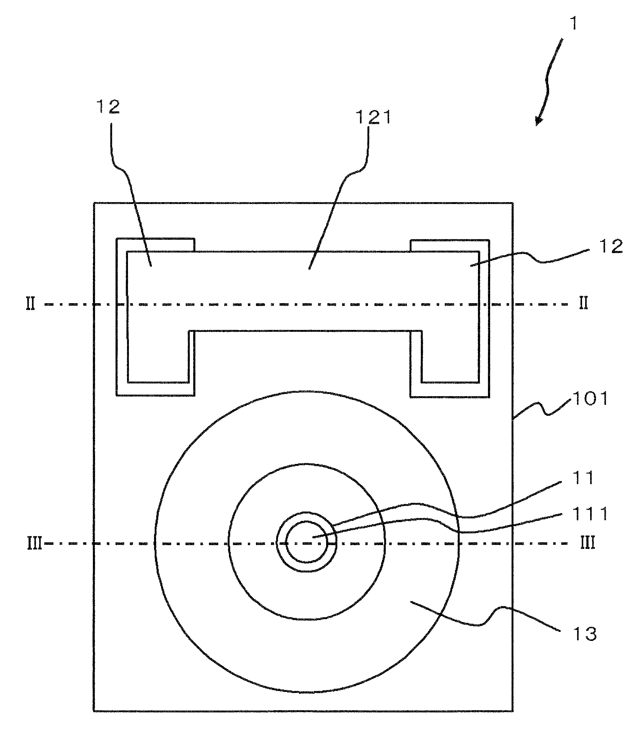
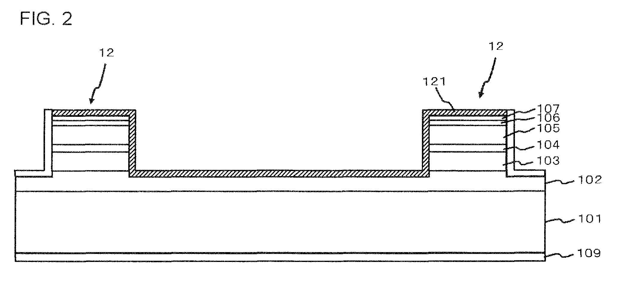
In FIG. 1 to FIG. 3, a semiconductor optical element is shown. In this embodiment, the semiconductor optical element is a semiconductor light receiving element 1. FIG. 1 is a plan view of the light receiving element 1, and FIG. 2 is a sectional view taken along direction II-II in FIG. 1. FIG. 3 is a sectional view taken along direction III-III in FIG. 1.

First, an outline of the light receiving element 1 will be explained.

The light receiving element 1 has a semiconductor substrate 101, a first mesa 11 provided over the semiconductor substrate 101, and having an active region and a first electrode (p-side electrode 111) provided over the active region; second mesas 12 provided over the semiconductor substrate 101, and each having a semiconductor layer and a second electrode (n-side electrode 121) provided over the semiconductor layer; and a third mesa 13 provided over the semiconductor substrate 101, and having a semiconductor layer, wherein the third mesa 13 is arranged so as to surr...

second embodiment

A second embodiment will be explained referring to FIG. 5 to FIG. 7.

FIG. 5 is a plan view of a light receiving element 3, and FIG. 6 is a sectional view taken along direction VI-VI in FIG. 5. FIG. 7 is a plan view of a substrate for mounting 4 on which the light receiving element 3 is mounted.

As shown in FIG. 5 and FIG. 6, the light receiving element 3 of this embodiment is different from the first embodiment in that a third mesa 33 has an extractor electrode 331 formed on the top thereof, and in that an interconnect 34, connecting the p-side electrode 111 on the top of the first mesa 11 and the extractor electrode 331 on the top of the third mesa 33, is provided.

Other aspects are same as those in the first embodiment.

The light receiving element 3 will be detailed below.

The light receiving element 3 has the first mesa 11 and the second mesas 12 which are similar to those in the above-described embodiment. The light receiving element 3 has also a third mesa 33.

The third mesa 33 is co...

third embodiment

A semiconductor optical element of this embodiment will be explained referring to FIG. 8 to FIG. 10.

The semiconductor optical element was a light receiving element in each of the above-described embodiments, whereas it is a semiconductor light emitting element in this embodiment.

FIG. 8 is a plan view of a light emitting element 5 of this embodiment, and FIG. 9 is a sectional view taken along direction IX-IX in FIG. 8. FIG. 10 is a sectional view taken along direction X-X in FIG. 8.

The light emitting element 5 is a surface emission semiconductor laser element of vertical oscillator type, and has a semiconductor substrate 501, and a semiconductor layer provided over the semiconductor substrate 501.

The semiconductor substrate 501 is typically an n-type GaAs substrate.

As shown in FIGS. 9, 10, the semiconductor layer is composed of an n-side, multi-layered reflective film 502, an active layer (light emitting layer, active region) 503, a current confining layer 504, a p-side, multi-layere...


PUM


Abstract

A light receiving element 1 has a semiconductor substrate 101; a first mesa 11 provided over the semiconductor substrate 101, and having an active region and a first electrode (p-side electrode 111) provided over the active region; a second mesa 12 provided over the semiconductor substrate 101, and having a semiconductor layer and a second electrode (n-side electrode 121) provided over the semiconductor layer; and a third mesa 13 provided over the semiconductor substrate 101, and having a semiconductor layer, wherein the third mesa 13 is arranged so as to surround the first mesa 11.

Description

TECHNICAL FIELDThe present invention relates to a semiconductor optical element.BACKGROUND ARTWith explosive increase in needs of wide-band multi media communication service such as the Internet, there has been an expectation on development of an optical fiber communication system having a large capacity and advanced functions. The number of optical communication modules used for such large-sized system has steadily been increasing with megasizing of the system, so that cost and load of mounting, as well as size of the optical communication modules, have become no more ignorable relative to the entire system. Therefore, downsizing of the optical communication modules per se, integration of functions, and cost reduction are understood as being most critical subjects.In particular, hybrid optical integrated module, having semiconductor optical elements mounted by flip-chip bonding onto a platform having an optical waveguide circuit preliminarily formed thereon, is strongly expected as...

Claims


Application Information

Patent Timeline
Patent Type & Authority Patents(United States)
IPC IPC(8): H01L29/06H01L33/20
CPCH01L31/022408H01L31/035281H01L31/109H01L33/20H01L31/1075Y02E10/50
Inventor WATANABE, SAWAKISHIBA, KAZUHIRONAKATA, TAKESHI
Owner NEC CORP
Why Eureka
Try Eureka