Display driver and display driving method
a technology of display driver and display device, applied in the field of display driver, can solve the problems of increasing power consumption and mpu load, affecting the display effect, so as to prevent the display of images with image distortion
- Summary
- Abstract
- Description
- Claims
- Application Information
AI Technical Summary
Benefits of technology
Problems solved by technology
Method used
Image
Examples
first embodiment
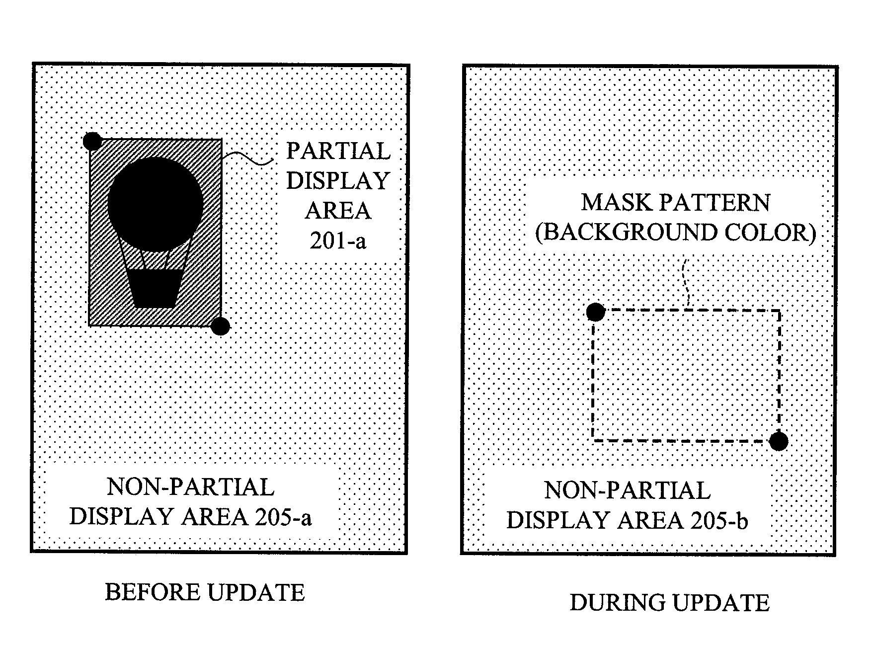
[0027]A display driver and a driving method of an active-matrix display device according to a first embodiment of the present invention will be described with reference to FIG. 1 to FIG. 3. In this case, although a liquid crystal display device is described as one example of the active-matrix display device, it is applicable to other display devices such as organic EL display.
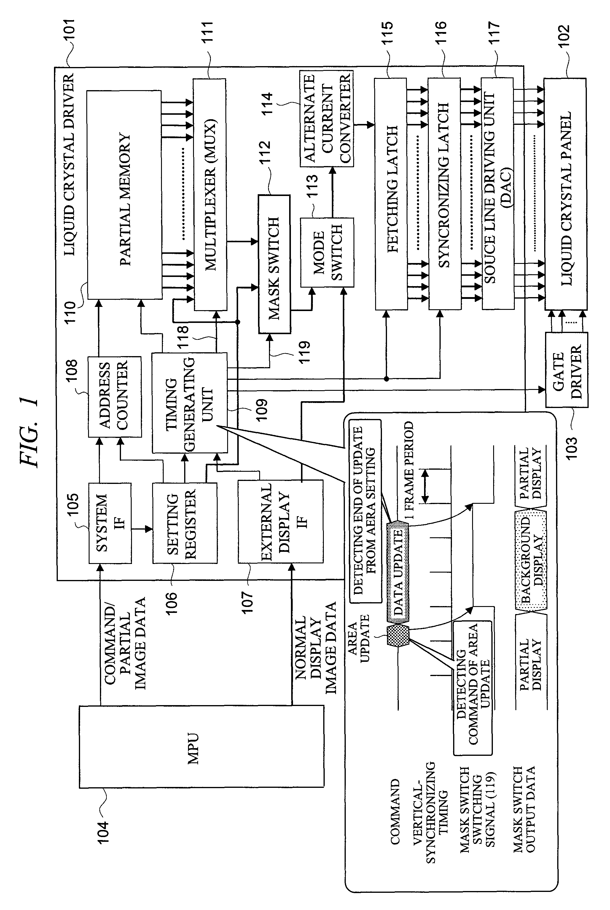
[0028]FIG. 1 shows a block diagram showing a liquid crystal driver of a liquid crystal display according to the first embodiment of the present invention and a connection relation with external devices thereof.
[0029]In FIG. 1, 101 indicates a liquid crystal driver as the display driver of the present invention, 102 indicates a liquid crystal panel of a so-called active-matrix type, in which liquid crystal pixels are each connected to a data line via a thin film transistor (TFT) and sandwiched between a pixel electrode and a common electrode are arranged on intersections of a plurality of scanning lines and a pl...
second embodiment
[0055]A display device according to a second embodiment of the present invention will be described with reference to FIG. 4.
[0056]FIG. 4 shows a liquid crystal driver of a liquid crystal display according to the second embodiment of the present invention and a connection relation with an external device thereof.
[0057]In the second embodiment, its block configuration is the same with FIG. 1 referred in the first embodiment and its operation is similar to that of the first embodiment. At the same time, a mask-switch-switching signal 119-a which controls the mask switch 112 as the switching means of the present invention is generated, and so it is a difference from the mask-switch-switching signal 119 in the first embodiment. Accordingly, the generation of the mask-switch-switching signal 119-a will be described.
[0058]The mask switch is controlled by the mask-switch-switching signal 119-a at the timing when receiving the mask validation command and the mask cancel command from the MPU ...
third embodiment
[0063]A display device according to a third embodiment will be described with reference to FIG. 5.
[0064]FIG. 5 shows a block configuration of a liquid crystal driver of a liquid crystal display according to the third embodiment of the present invention and a connection relation with external devices thereof.
[0065]In the third embodiment, the mask switch 112 in FIG. 1 (first embodiment) and FIG. 4 (second embodiment) is used for both functions of switching partial validation period and the background pattern. Meanwhile, other operations and effects are the same with those of the first embodiment and the second embodiment.
[0066]In the third embodiment, a control-signal-masking circuit 301 as a masking means is added, which masks the partial-display timing 118 by the mask-switch-switching signal 119 and generates partial-display timing 118-a which does not validate displaying when updating the partial-display data. The control signal masking circuit 301 generates the partial-display ti...
PUM
 Abstract
Description
Claims
Application Information


