Method and device for scanning light

a light scanning and light technology, applied in the field of light scanning, can solve the problems of large power consumption, system limitations, bulky crts, etc., and achieve the effect of high quality

Active Publication Date: 2011-05-31
APPLE INC
View PDF4 Cites 124 Cited by
  • Summary
  • Abstract
  • Description
  • Claims
  • Application Information

AI Technical Summary

Benefits of technology

[0081]According to still further features in the described preferred embodiments a shape of the first and / or second micromirrors is selected so as to minimize a moment-of-inertia thereof.
[0101]According to still further features in the described preferred embodiments the method further comprises applying a reflective coat on the micromirror so as to improve a reflectivity thereof.
[0118]The present invention successfully addresses the shortcomings of the presently known configurations by providing a scanning method and scanning device capable of providing high quality images far exceeding prior art technologies.

Problems solved by technology

Such systems suffer from several limitations.
CRTs are bulky and consume substantial amounts of power hence being undesirable for small-scale applications such as head-mounted or retinal displays.
Additionally, the manufacturing cost of CRTs is proportional to the display area thus making them undesirable for large-scale applications such as large screen video projectors.
It is recognized that this limits the ability of larger CRTs to produce fine details.
However, similarly to the CRT, flat panel displays become rather expensive for large-scale applications.
Conversely, typical flat panel displays utilize screens that are at least several inches across, hence being less favored for applications in which the display is intended to occupy only a small portion of a user's field of view.
However, the brightness and contrast are poor compared to that of a CRT used for home TV video viewing.
Although these projectors have fair resolution, there are other unavoidable problems related to this scheme.
The incandescent white light source has a relatively short operating life and generates relatively large amounts of heat.
The liquid crystal panel devices cannot be manufactured without some minimum number of defects that, in turn, manifest themselves as permanent image artifacts on the screen regardless of the graphic or video source.
Additionally, the use of liquid crystal panel introduces a fixed and permanent resolution to the display device, making it very difficult to adapt the electronics to accept other resolutions for display of graphics and text information
Mechanically, the image resolution is limited by the number of lines that one mirror can scan during the refresh period of another mirror.
Industrial attempts to integrate magnetic actuators within MEMS have encountered difficulties in maintaining optimal values of force, temperature or efficiency.
The disadvantage of this method is nonlinearity of the actuation, in particular when relatively large motions are required.
Thermal actuators, however, induce large stresses which can cause severe problems for long term reliability.
A major drawback of these devices is a fast wear and fatigue of the shape memory alloys, compared to brittle materials.
One limitation of piezoelectric actuators is that the actuation distance is relatively small, typically no more than a few percents of the total length of the piezoelectric material.
In addition, piezoelectric actuators generate a considerable amount of heat which reduces the actuation efficiency.
Irrespective of the mechanism which is responsible to the motion of the mirrors, prior art display systems fail to provide high resolution in both the horizontal and vertical directions as demanded by many applications.
For example, one difficulty with prior art displays is a raster pinch, where, due to differences between the actual scan pattern and the optimal raster scan pattern, successive forward and reverse sweeps of the beam results in unevenly spacing of the pixels at several points of the scan pattern.
This uneven spacing can cause the pixels to overlap or can leave a gap between adjacent rows of pixels.
Moreover, because image information is typically provided as an array of data, where each location in the array corresponds to a respective position in the ideal raster pattern, the displaced pixel locations can cause image distortion.

Method used


Image

  • Method and device for scanning light
  • Method and device for scanning light
  • Method and device for scanning light

Examples


example

[0192]Reference is now made to the following example, which together with the above descriptions illustrates the invention in a non limiting fashion.

MEMS Manufacturing Process

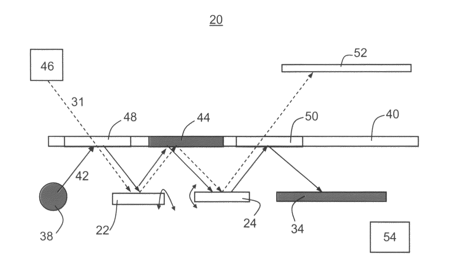
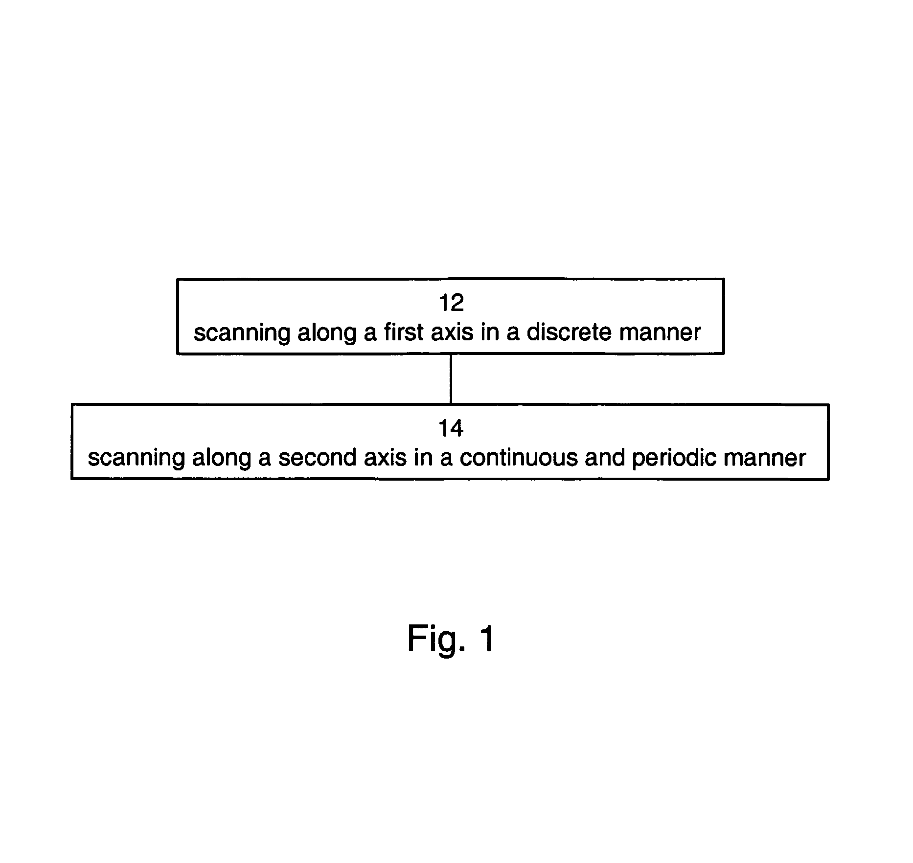
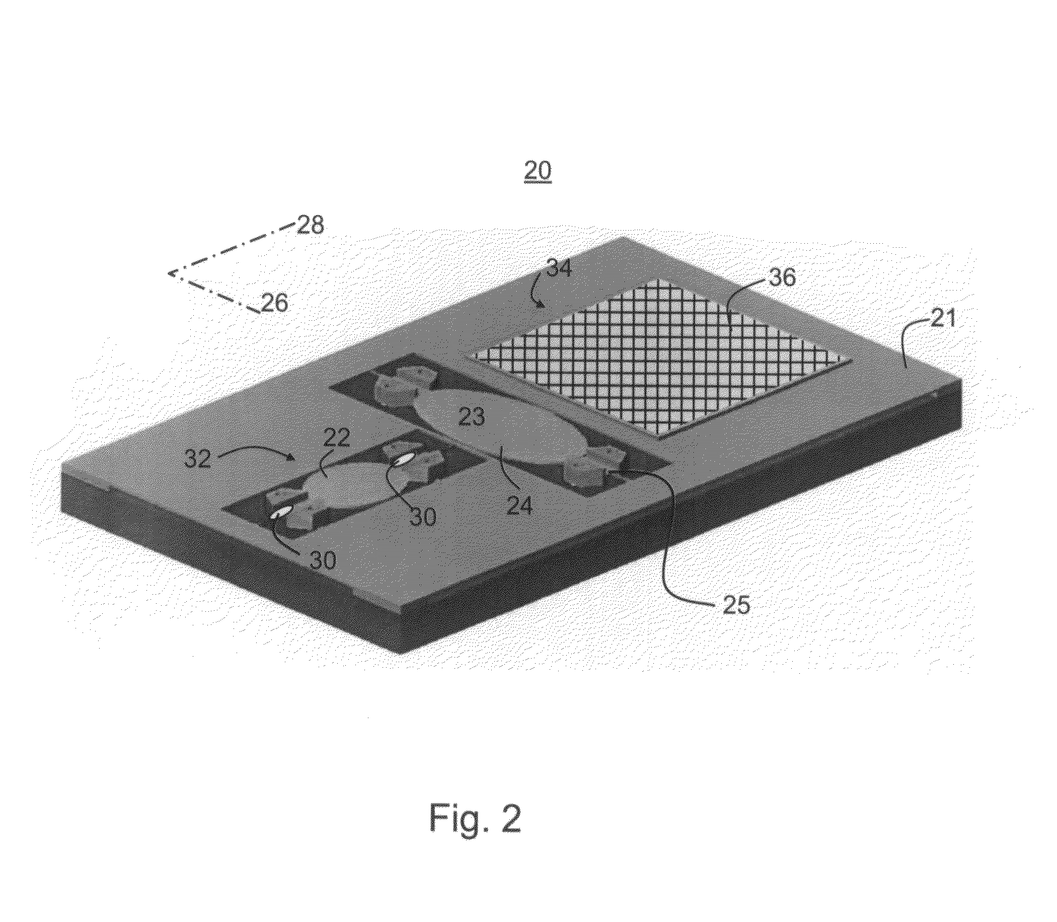
[0193]As stated, the dimension of any component of device 20 is preferably in the sub-millimeter range, in which case device 20 preferably comprises a MEMS. Thus, according to a preferred embodiment of the present invention there is provided a method of manufacturing a MEMS. The method comprises the following method steps which are illustrated in the flowchart of FIG. 6. Block 82 represents a step in which a rotor assembly having a permanent magnet is manufactured, and Block 84 represents a step in which a stator assembly having an arrangement of coils is manufactured. Preferred manufacturing processes of the stator assembly and the rotor assembly are further detailed hereinunder. The manufacturing processes represented by Blocks 82 and 84 can be performed either sequentially or contemporaneously. In an additio...


PUM

PropertyMeasurementUnit
thicknessesaaaaaaaaaa

Abstract

A method of scanning a light beam is disclosed. The method comprises scanning the light beam along a first axis and scanning the light beam along a second axis, such that a functional dependence of the scanning along the first axis is substantially a step-wave, and a functional dependence of the scanning along the second axis is other than a step-wave.

Description

RELATED APPLICATIONS[0001]This Application is a National Phase of PCT Patent Application No. PCT / IL2005 / 001194 having International Filing Date of Nov. 14, 2005, which claims the benefit of Israel Patent Application No. 165212 filed on Nov. 15, 2004. The contents of the above Applications are all incorporated herein by reference.FIELD AND BACKGROUND OF THE INVENTION[0002]The present invention relates to light scanning and, more particularly, to a scanning method and device for providing images.[0003]A variety of techniques are available for providing visual displays of graphic or video images to a user. The most familiar of these techniques involves the use of a cathode ray tube (CRT), such as in television displays and monitor displays, which provide images by scanning electron beams. Generally, in such displays the image is uniformly decomposed into a number of picture elements (e.g., pixels) typically of the same size, whereby imagery information (for example, colors and brightne...

Claims


Application Information

Patent Timeline
Patent Type & Authority Patents(United States)
IPC IPC(8): G02B26/08G02BH04N3/08
CPCH04N3/08G02B26/085G02B26/105G02B26/121G02B26/101Y10T29/49012Y10T29/49009
Inventor WEISS, YIZHARVELGER, MORDEKHAINATAN-KNAZ, SIVANERLICH, RAVIVSROMIN, ALEXANDER
Owner APPLE INC
Why Eureka
Try Eureka