Image detector and radiation detecting system with separation of metal layers for bias, scan and data lines

a radiation detection system and metal layer separation technology, applied in the field of image detectors, can solve the problems of deteriorating loss of storage capacitor lines, scan lines, etc., and achieve the effects of improving the production yield of tft arrays, reducing electronic noise, and improving image quality of detected images

Active Publication Date: 2011-06-07
FUJIFILM CORP
View PDF9 Cites 13 Cited by
  • Summary
  • Abstract
  • Description
  • Claims
  • Application Information

AI Technical Summary

Benefits of technology

[0043]According to the first aspect of the invention, the scan lines, data lines and common lines are each formed by metal layers that are different from each other and that have been provided with respective insulating film therebetween, therefore the production yield of the TFT array may be improved. Furthermore, since electronic noise may be reduced, the image quality of detected images may be improved.

Problems solved by technology

In a radiation image detector configured as above, there are two important problems which need to be addressed, these being the drop in production yield of the TFT array and deterioration of the image quality of detected images.
However, line defects, including leakage of storage capacitor lines, scan lines, and data lines, are difficult to physically repair by laser repair or the like in the TFT array process, and also are difficult to rectify by image correction.
Therefore, line defects are critical defects and are a cause of increased production costs for TFT arrays.
Therefore, patterning defects occur when forming the gate layer, and if conductive material remains between the storage capacitor line and either the scan lines or the gate electrodes, leak may occur between the scan lines and the storage capacitor lines.
Such defects occur more frequently as the resolution of the image detector gets finer.

Method used


Image

  • Image detector and radiation detecting system with separation of metal layers for bias, scan and data lines
  • Image detector and radiation detecting system with separation of metal layers for bias, scan and data lines
  • Image detector and radiation detecting system with separation of metal layers for bias, scan and data lines

Examples


Embodiment Construction

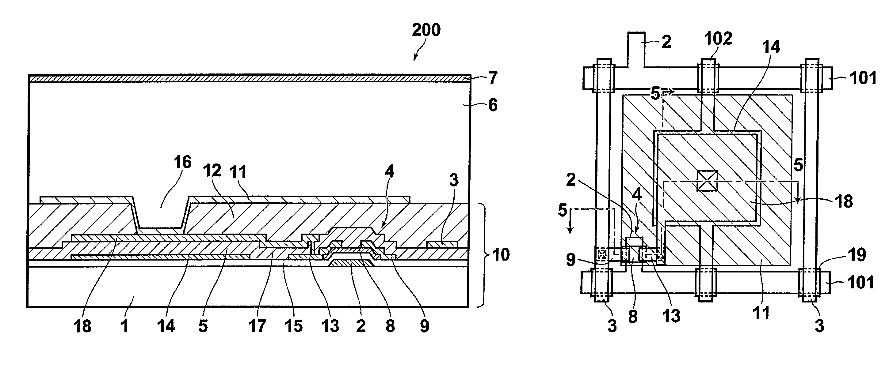
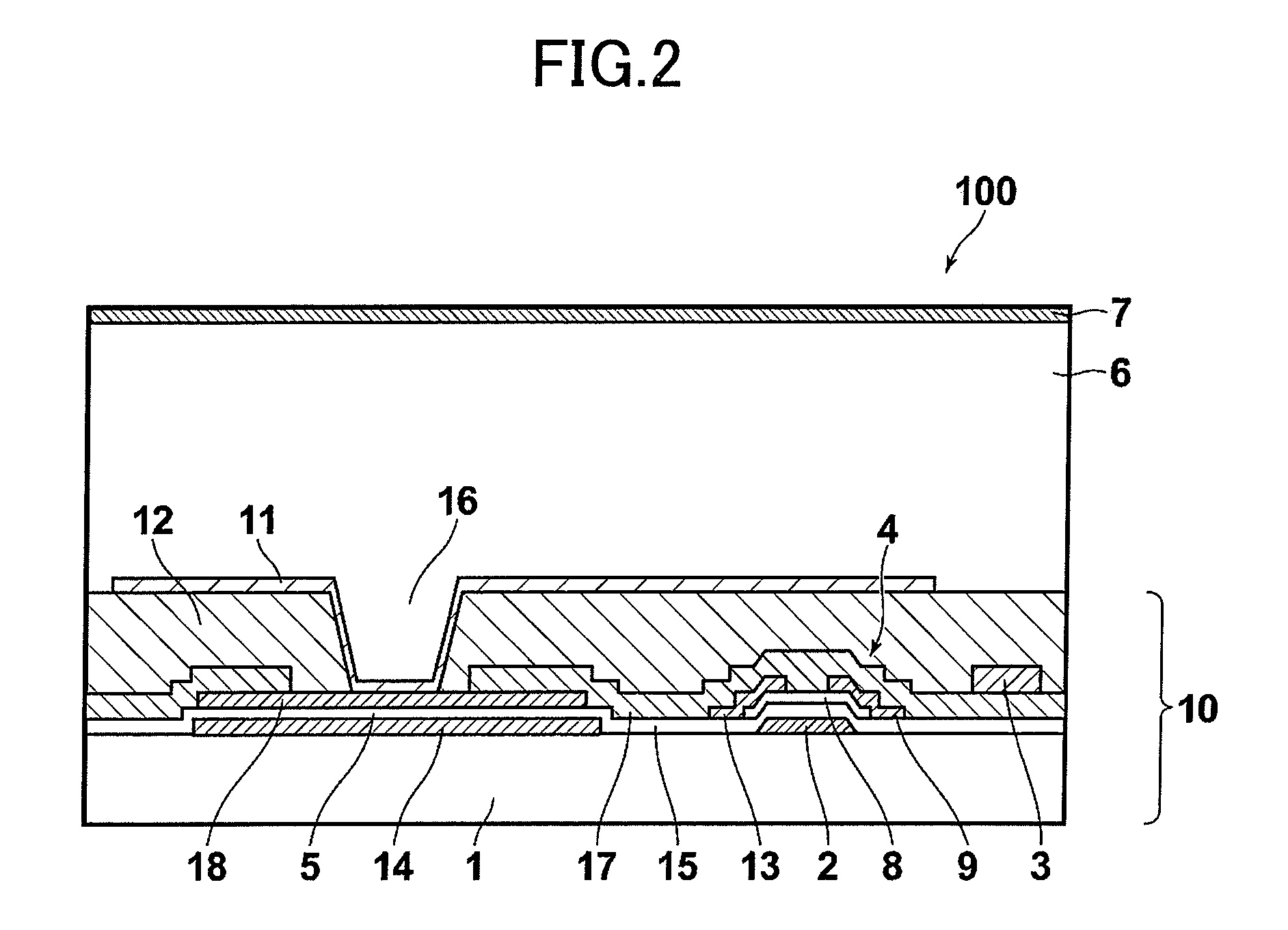
[0068]A radiation image detector to which one exemplary embodiment of an image detector of the invention is applied will be explained below with reference to the drawings.

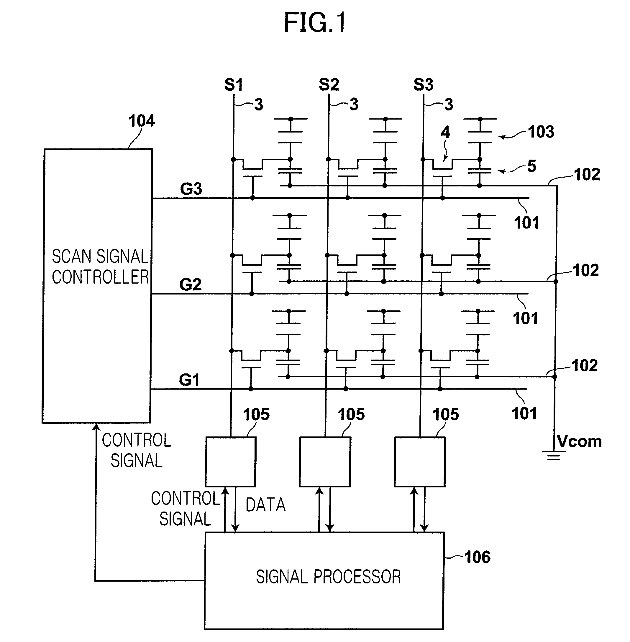
[0069]FIG. 1 is an equivalent circuit of the radiation image detector according to a first exemplary embodiment of the invention.

[0070]The radiation image detector of the first exemplary embodiment includes a large number of pixels arrayed two-dimensionally, each composed of an image sensor section 103 composed of a bias electrode, a semiconductor film and a charge collecting electrode as described later, a charge storage capacitor 5 for storing charge signals detected by the image sensor section 103 and a thin film transistor (referred to as a “TFT transistor” hereinafter) 4 for reading charges stored in the charge storage capacitor 5. Still more, there are provided a large number of scan lines 101 for turning ON / OFF the TFT switch 4 and a large number of data lines 3 for reading the charges stored in the charge s...


PUM


Abstract

The invention provides an image detector capable of improving the quality of detected images by reducing electronic noise, the image detector comprising, a plurality of scan lines disposed in parallel, a plurality of data lines provided so as to cross with the scan lines, thin film transistors connected with the scan and data lines and provided in matrix, sensor sections connected to the thin film transistor and provided in a matrix and a plurality of common lines disposed so as to apply bias voltage commonly to the sensor sections provided in matrix. Each of the scan lines, data lines and common lines are formed by metal layers different from each other and provided with insulating film(s) disposed therebetween.

Description

CROSS-REFERENCE TO RELATED APPLICATION[0001]This application claims priority under 35 USC 119 from Japanese Patent Application No. 2006-342754 and 2007-324263, the disclosure of which is incorporated by reference herein.BACKGROUND OF THE INVENTION[0002]1. Field of the Invention[0003]The present invention relates to an image detector in which a large number of pixels having a thin film transistor is two-dimensionally arrayed and specifically relates to a structure of the pixel thereof.[0004]2. Description of the Related Art[0005]A FPD (Flat Panel Detector) in which an X-ray sensitive layer is disposed on a TFT active matrix substrate and is capable of converting X-ray information directly into digital data, has been put into practice lately. The FPD has merit that enables one to instantly confirm images and even video images as compared to a prior art imaging plate. Therefore, it is spreading rapidly.[0006]At first, radiation image detector using the FPD will be explained with refere...

Claims


Application Information

Patent Timeline
Patent Type & Authority Patents(United States)
IPC IPC(8): H01L31/00
CPCH01L27/14603H01L27/14632H01L27/14692H01L27/14676
Inventor OKADA, YOSHIHIROYOSHIMI, TAKUYA
Owner FUJIFILM CORP
Why Eureka
Try Eureka