Method for the manufacture of electronic devices on substrates and devices related thereto

a technology of electronic devices and substrates, applied in the field of electronic devices, can solve the problems of increasing the operating voltage of solar cell arrays, and increasing the mass of such arrays

Inactive Publication Date: 2011-06-14
INTERUNIVERSITAIR MICRO ELECTRONICS CENT (IMEC VZW) +1
View PDF14 Cites 70 Cited by
  • Summary
  • Abstract
  • Description
  • Claims
  • Application Information

AI Technical Summary

Problems solved by technology

However, increasing operating voltage for current solar arrays could result in a significant increase in the mass of such arrays.
Such an increase in mass is inconsistent with a general desire to reduce the overall mass of spacecraft.
Furthermore, increasing a solar cell array's operating voltage also increases the likelihood of degradation of the solar cell array due to arcing that may occur as a result of plasma-prone environments, especially those that exist in spacecraft environments.

Method used


Image

  • Method for the manufacture of electronic devices on substrates and devices related thereto
  • Method for the manufacture of electronic devices on substrates and devices related thereto
  • Method for the manufacture of electronic devices on substrates and devices related thereto

Examples


example device

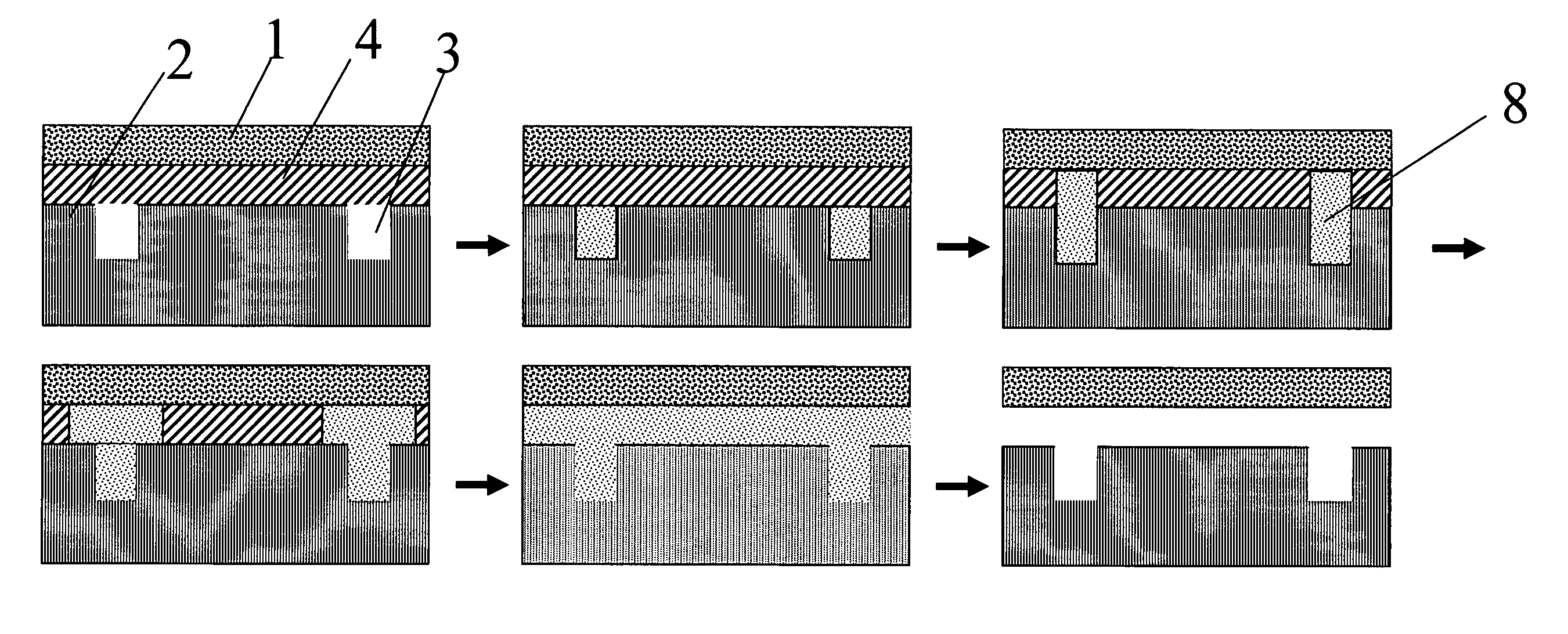
[0058]FIG. 6 is a drawing that illustrates the device substrate 1 and carrier substrate 7, which are bonded with the bonding agent 6, after release from the carrier substrate 2, such as by using a process such as the process described with respect to FIG. 5. Electronic devices are formed on (and / or in) the device substrate 1. The devices include the electrical connections 5. The electronic devices formed on the surface of (and / or in) the device substrate 1 may include solar cells, light-emitting diodes, CMOS circuits or any other device achievable by semiconductor processing, or the like. Further processing may now occur on the surface of the device substrate 1 that was previously bonded with the carrier substrate 2. Mechanical support and stability during such processing will be provided by the carrier substrate 7 in conjunction with the bonding agent 6.

Empirical Example

[0059]The following is an empirical example applying an embodiment of the methods described herein. In this examp...


PUM


Abstract

Methods for manufacturing electronic devices and devices produced by those methods are disclosed. One such method includes releasably bonding a first surface of a device substrate to a face of a first carrier substrate using a first bonding agent to produce a first composite substrate, where the face of the first carrier substrate includes a pattern of trenches. The method also includes processing the device substrate to manufacture an electronic device on a second surface of the device substrate. The method further includes releasing the device substrate from the first carrier substrate by a releasing agent.

Description

CROSS REFERENCE TO RELATED APPLICATIONS[0001]This application claims priority benefit under 35 U.S.C. §119(e) to U.S. Provisional Patent Application Ser. No. 60 / 577,162, filed on Jun. 4, 2004. This application also claims foreign priority benefit under 35 U.S.C. §119(a) to European Patent Application EP 04447140.7, filed on Jun. 8, 2004. The disclosures of U.S. Provisional Patent Application Ser. No. 60 / 577,162 and European Patent Application EP 04447140.7 are incorporated by reference herein in their entirety.BACKGROUND[0002]1. Field[0003]This disclosure relates to electronic devices and, more particularly, to methods for manufacturing electronic devices on substrates and devices produced by those methods.[0004]2. Description of Related Art[0005]Solar cell arrays are often used in space exploration application to provide a source of power for equipment used in such applications. As the exploration of space continues to advance, the power production requirements for solar arrays use...

Claims


Application Information

Patent Timeline
Patent Type & Authority Patents(United States)
IPC IPC(8): H01L21/30H01L21/46H01L21/20H01L21/68H01L31/00H01L31/05H01L31/18
CPCH01L21/2007H01L31/182B64G1/443H01L31/0508H01L31/1896H01L2221/68318H01L2221/68363Y02P70/521Y02E10/546Y02P70/50
Inventor FLAMAND, GIOVANNIGEENS, WIMPOORTMANS, JEF
Owner INTERUNIVERSITAIR MICRO ELECTRONICS CENT (IMEC VZW)
Why Eureka
Try Eureka