Package in package semiconductor device

Active Publication Date: 2011-07-19
AMKOR TECH SINGAPORE HLDG PTE LTD
View PDF469 Cites 50 Cited by
  • Summary
  • Abstract
  • Description
  • Claims
  • Application Information

AI Technical Summary

Benefits of technology

[0008]In accordance with the present invention, there is provided multiple embodiments of a package-in-package semiconductor device including shortened electrical signal paths to optimize electrical performance. In each embodiment, the semiconductor device comprises a substrate having a conductive pattern formed thereon. In certain embodiments, a semiconductor package and one or more semiconductor dies are vertically stacked upon the substrate, and placed into electrical communication with the conductive pattern thereof. One or more of the semiconductor dies may include through-silicon vias formed therein for facilitating the electrical connection thereof to the conductive pattern of the substrate or to other electronic co

Problems solved by technology

In the currently known PIP device configurations, and particularly those in which the electronic components are vertically stacked (i.e., extend perpendicularly relative to the substrate), the electrical signal paths in the PIP device are inevitably lengthened, thus resulting in a deterioration in the electrical performance of the PIP device.
Further, the use of a large number of conductive wires leads to a high probability of shorting between the conductive wires in the encapsulation step described above as used to form the package body of the PIP device.
Still further, in the event an increased number of electronic components are included in the PIP device, the design of the electrically conductive patterns on the substrate as needed to accommodate the conductive wires can be highly complex, thus adding to the difficulty in the fabrication of the PIP device and increasing the cost thereof.

Method used


Image

  • Package in package semiconductor device
  • Package in package semiconductor device
  • Package in package semiconductor device

Examples


first embodiment

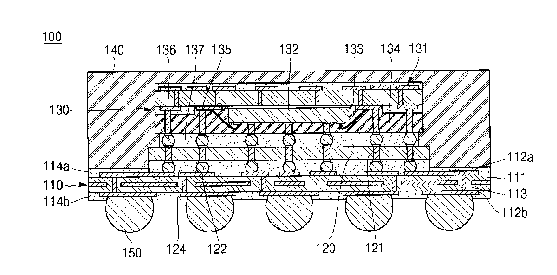
[0027]Referring now to the drawings wherein the showings are for purposes of illustrating various embodiments of the present invention and not for purposes of limiting the same, FIG. 1 depicts in cross-section a package-in-package semiconductor device 100 constructed in accordance with the present invention. The semiconductor device 100 comprises a substrate 110 which preferably has a generally quadrangular configuration. The substrate 110 can be selected from common circuit boards (e.g., rigid circuit boards and flexible circuit boards) and equivalents thereof. In this regard, the present invention is not intended to be limited to any particular type of substrate 110. By way of example and not by way of limitation, the substrate 110 may include an insulating layer 111 having opposed, generally planar top and bottom surfaces. Disposed on the top surface is an electrically conductive pattern 112a, while disposed on the bottom surface is an electrically conductive pattern 112b. The co...

second embodiment

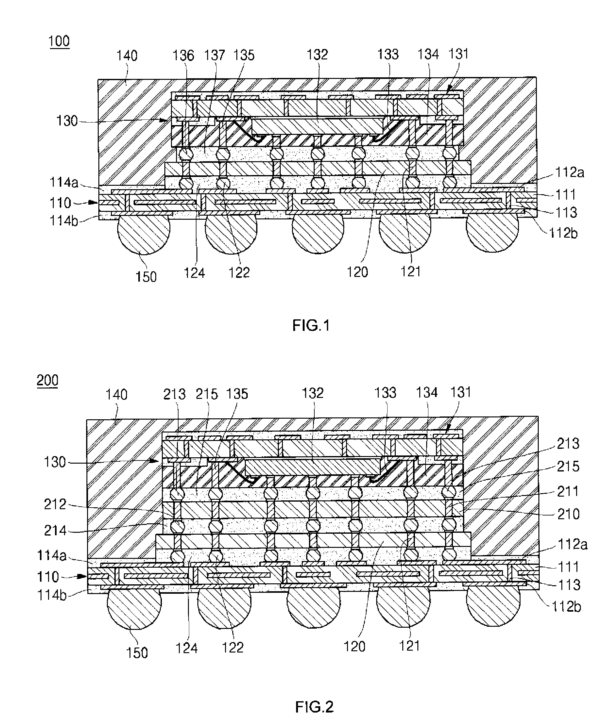
[0035]Referring now to FIG. 2, there is shown a semiconductor device 200 constructed in accordance with the present invention. The semiconductor device 200 is substantially similar to the above-described semiconductor device 100, with only the differences between the semiconductor devices 200, 100 being described below.

[0036]The sole distinction between the semiconductor devices 200, 100 lies in the addition of a second (middle) semiconductor die 210 to the semiconductor device 200. The second semiconductor die 210 is identically configured to the first semiconductor die 120, and includes a plurality of through-silicon vias 211 formed therein. Each of the vias 211 of the second semiconductor die 210 is filled with a conductive material in the same manner as the vias 121 of the first semiconductor die 120. Additionally, as seen in FIG. 2, the vias 211 of the second semiconductor die 210 are electrically connected to respective ones of the vias 121 of the first semiconductor die 120 t...

third embodiment

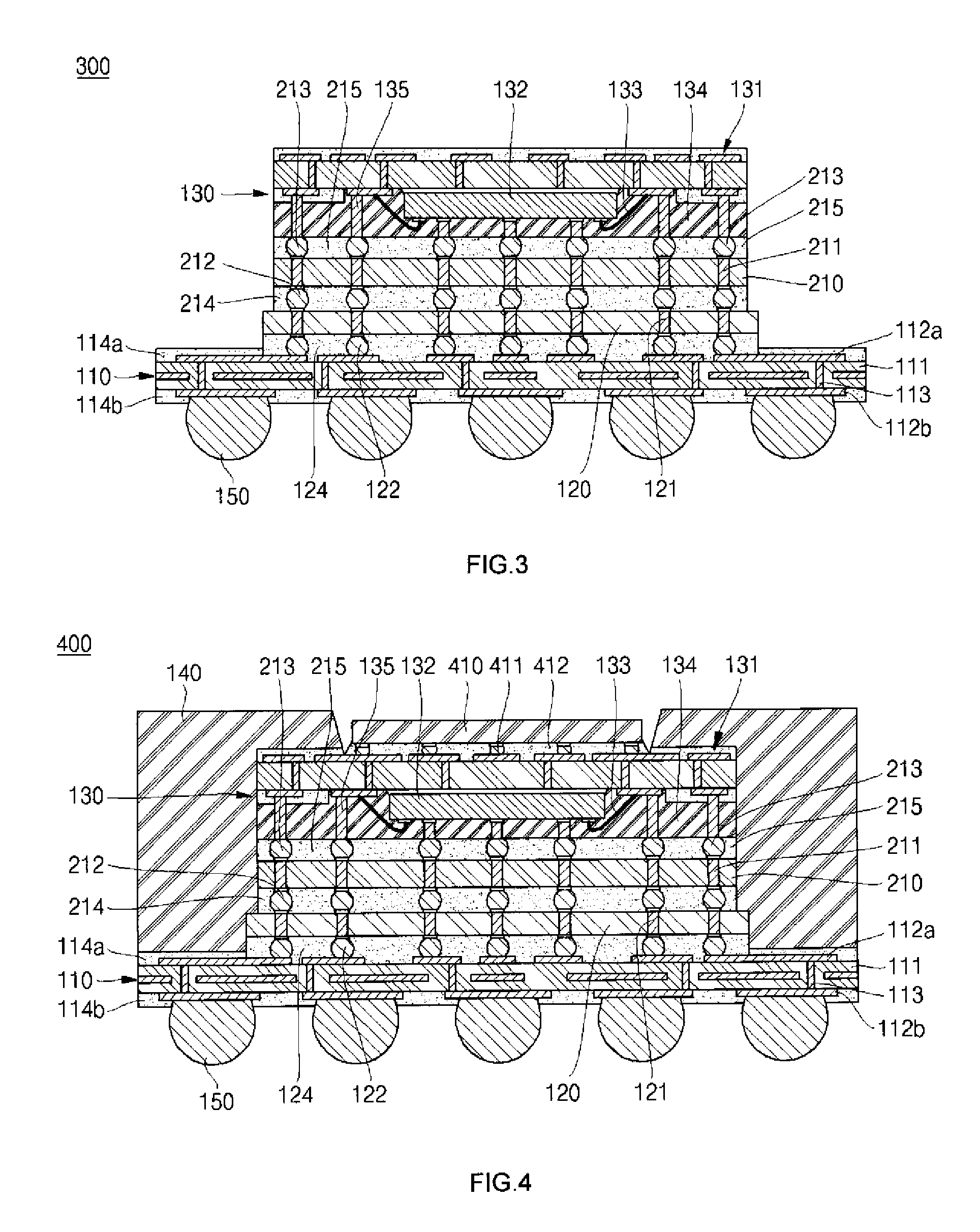
[0039]Referring now to FIG. 3, there is shown a semiconductor device 300 constructed in accordance with the present invention. The semiconductor device 300 is substantially similar to the above-described semiconductor device 200, with only the differences between the semiconductor devices 300, 200 being described below.

[0040]The sole distinction between the semiconductor devices 300, 200 lies in the omission of the package body 140 in the semiconductor device 300. As a result, in the semiconductor device 300, the first and second semiconductor dies 120, 210, as well as the semiconductor package 130, are each exposed. With this particular configuration, the semiconductor device 300 is able to exhibit improved heat sink performance in comparison to the semiconductor device 200.


PUM


Abstract

In accordance with the present invention, there is provided multiple embodiments of a package-in-package semiconductor device including shortened electrical signal paths to optimize electrical performance. In each embodiment, the semiconductor device comprises a substrate having a conductive pattern formed thereon. In certain embodiments, a semiconductor package and one or more semiconductor dies are vertically stacked upon the substrate, and placed into electrical communication with the conductive pattern thereof. One or more of the semiconductor dies may include through-silicon vias formed therein for facilitating the electrical connection thereof to the conductive pattern of the substrate or to other electronic components within the vertical stack. Similarly, the semiconductor package may be provided with through-mold vias to facilitate the electrical connection thereof to other electronic components within the vertical stack. In other embodiments of the present invention, a semiconductor die which is electrically connected to the conductive pattern of the substrate is encapsulated with an inner package body which itself is formed to include through-mold vias used to facilitate the electrical connection thereof to another semiconductor die stacked thereon. In each embodiment of the semiconductor device, the vertically stacked electronic components thereof may be covered with a package body which also partially covers the substrate.

Description

CROSS-REFERENCE TO RELATED APPLICATIONS[0001]Not ApplicableSTATEMENT RE: FEDERALLY SPONSORED RESEARCH / DEVELOPMENT[0002]Not ApplicableBACKGROUND OF THE INVENTION[0003]1. Field of the Invention[0004]The present invention relates generally to semiconductor devices, and more particularly to a package-in-package (PIP) semiconductor device having optimized electrical signal paths to provide enhanced electrical performance.[0005]2. Description of the Related Art[0006]Package-in-package (PIP) semiconductor devices are currently known and used in the electrical arts. A typical PIP semiconductor device comprises various combinations of electronic components including passive devices, semiconductor dies, semiconductor packages, and / or other elements which are arranged in a horizontal direction, or stacked in a vertical direction on an underlying substrate. In many PIP devices, the substrate and the electronic components are interconnected to one another through the use of conductive wires alon...

Claims


Application Information

Patent Timeline
IPC IPC(8): H01L23/48
CPCH01L25/03H01L23/3121H01L24/16H01L2224/0557H01L2224/14181H01L2224/0401H01L2924/0002H01L2924/19107H01L2224/32145H01L2224/16225H01L2224/16145H01L2224/13025H01L2924/01322H01L2924/15311H01L2924/01079H01L2225/06572H01L2225/06541H01L2225/06517H01L2225/06513H01L2224/73265H01L2224/73204H01L2224/48227H01L2224/48091H01L2224/32225H01L24/32H01L24/73H01L2924/00014H01L2924/00H01L2924/00012H01L2224/05552H01L2224/73209H01L2224/17181
Inventor KANG, DAE BYOUNGYANG, SUNG JINOK, JUNG TAEKIM, JAE DONG
Owner AMKOR TECH SINGAPORE HLDG PTE LTD
Why Eureka
Try Eureka