Package in package semiconductor device with film over wire

a semiconductor device and film technology, applied in the field of semiconductor devices, can solve the problems of deteriorating the electrical performance of the pip device, high probability of shorting between the conductive wires, and high complexity of electrically conductive patterns on the substrate as needed to accommodate the conductive wires, so as to shorten the electrical signal path and optimize the electrical performance

Active Publication Date: 2013-07-16
AMKOR TECH SINGAPORE HLDG PTE LTD
View PDF420 Cites 6 Cited by
  • Summary
  • Abstract
  • Description
  • Claims
  • Application Information

AI Technical Summary

Benefits of technology

[0008]In accordance with the present invention, there is provided multiple embodiments of a package-in-package semiconductor device including shortened electrical signal paths to optimize electrical performance. The semiconductor device comprises a substrate having a conductive pattern formed thereon. In each embodiment of the semiconductor device, a semiconductor package and one or more semiconductor dies are vertically stacked upon the substrate, and placed into electrical communication with the conductive pattern thereof. In certain embodiments, a semiconductor die which is electrically connected to the conductive pattern of the substrate may be fully or partially covered with a film-over-wire. Additionally, in each embodiment of the semiconductor device, the vertically stacked electronic components thereof may be covered with a package body which also partially covers the substrate.

Problems solved by technology

In the currently known PIP device configurations, and particularly those in which the electronic components are vertically stacked (i.e., extend perpendicularly relative to the substrate), the electrical signal paths in the PIP device are inevitably lengthened, thus resulting in a deterioration in the electrical performance of the PIP device.
Further, the use of a large number of conductive wires leads to a high probability of shorting between the conductive wires in the encapsulation step described above as used to form the package body of the PIP device.
Still further, in the event an increased number of electronic components are included in the PIP device, the design of the electrically conductive patterns on the substrate as needed to accommodate the conductive wires can be highly complex, thus adding to the difficulty in the fabrication of the PIP device and increasing the cost thereof.

Method used


Image

  • Package in package semiconductor device with film over wire
  • Package in package semiconductor device with film over wire
  • Package in package semiconductor device with film over wire

Examples


first embodiment

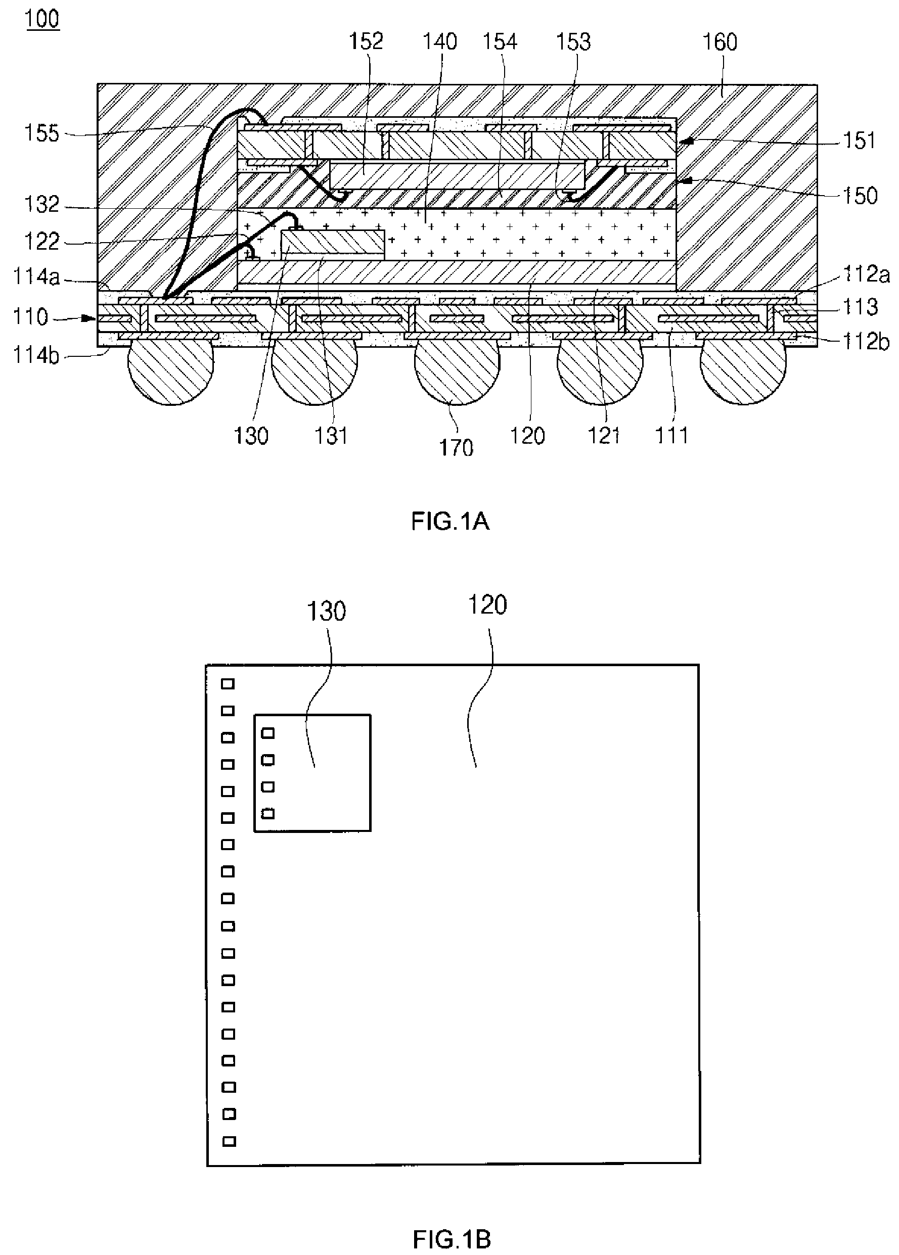
[0023]Referring now to the drawings wherein the showings are for purposes of illustrating various embodiments of the present invention and not for purposes of limiting the same, FIG. 1A depicts in cross-section a package-in-package semiconductor device 100 constructed in accordance with the present invention. The semiconductor device 100 comprises a substrate 110 which preferably has a generally quadrangular configuration. The substrate 110 can be selected from common circuit boards (e.g., rigid circuit boards and flexible circuit boards) and equivalents thereof. In this regard, the present invention is not intended to be limited to any particular type of substrate 110. By way of example and not by way of limitation, the substrate 110 may include an insulating layer 111 having opposed, generally planar top and bottom surfaces. Disposed on the top surface is an electrically conductive pattern 112a, while disposed on the bottom surface is an electrically conductive pattern 112b. The c...

second embodiment

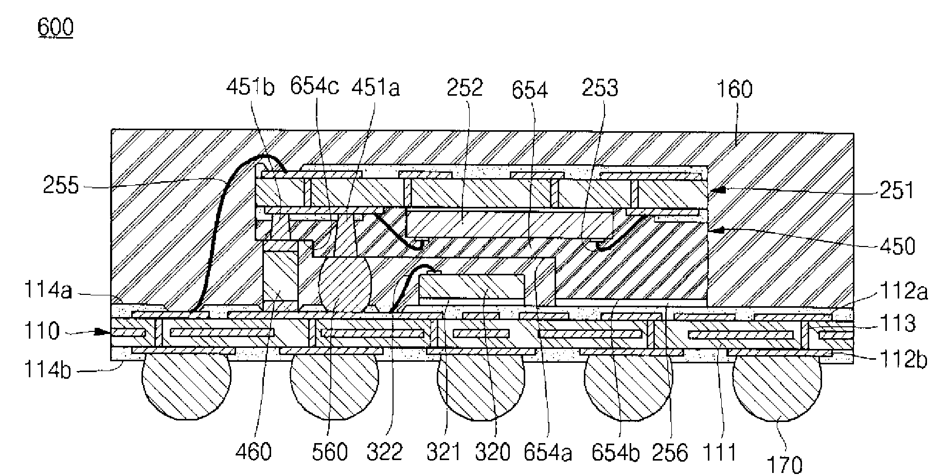
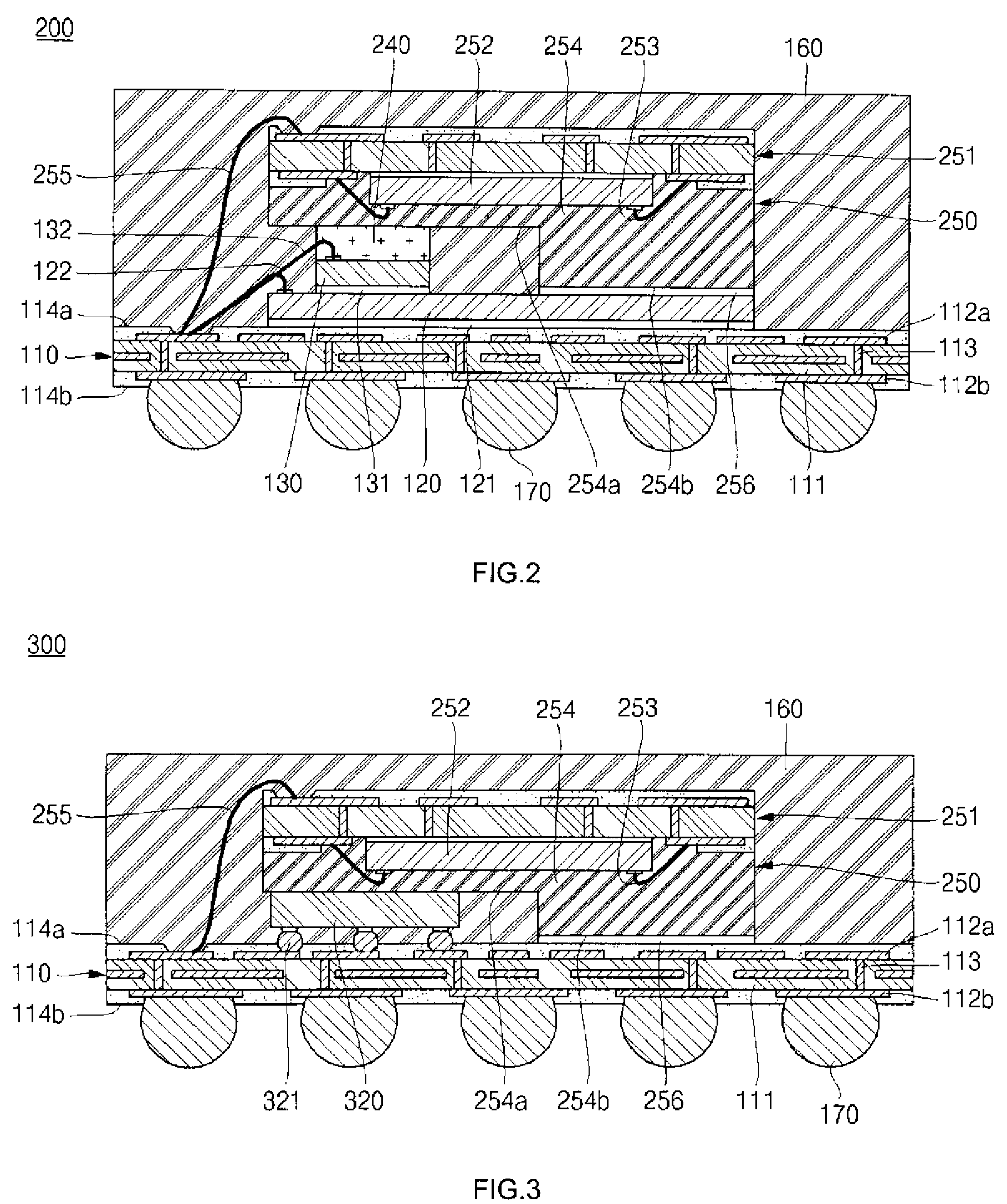
[0032]Referring now to FIG. 2, there is shown a semiconductor device 200 constructed in accordance with the present invention. The semiconductor device 200 is substantially similar to the above-described semiconductor device 100, with only the differences between the semiconductor devices 200, 100 being described below.

[0033]The primary distinction between the semiconductor devices 200, 100 lies in the substitution of the semiconductor package 150 of the semiconductor device 100 with the semiconductor package 250 in the semiconductor device 200. The semiconductor package 250 comprises an inner substrate 251 which includes an insulating layer defining opposed top and bottom surfaces and electrically conductive patterns formed on respective ones of the opposed top and bottom surfaces of the insulating layer. In the inner substrate 251, the conductive patterns disposed on respective ones of the opposed top and bottom surfaces of the insulating layer are electrically connected to each o...

third embodiment

[0038]Referring now to FIG. 3, there is shown a semiconductor device 300 constructed in accordance with the present invention. The semiconductor device 300 is also substantially similar to the above-described semiconductor device 200, with only the differences between the semiconductor devices 300, 200 being described below.

[0039]The primary distinction between the semiconductor devices 300, 200 lies in the elimination of the FOW 240 in the semiconductor device 300, and the substitution of the first and second semiconductor dies 120, 130 of the semiconductor device 200 with the first (bottom) semiconductor die 320 in the semiconductor device 300. More particularly, as seen in FIG. 3, the first semiconductor die 320 defines opposed, generally planar top and bottom surfaces, and includes a plurality of conductive contacts or terminals disposed on the bottom surface thereof. These terminals are electrically connected to the conductive pattern 112a of the substrate 110 through the use o...


PUM


Abstract

In accordance with the present invention, there is provided multiple embodiments of a package-in-package semiconductor device including shortened electrical signal paths to optimize electrical performance. The semiconductor device comprises a substrate having a conductive pattern formed thereon. In each embodiment of the semiconductor device, a semiconductor package and one or more semiconductor dies are vertically stacked upon the substrate, and placed into electrical communication with the conductive pattern thereof. In certain embodiments, a semiconductor die which is electrically connected to the conductive pattern of the substrate may be fully or partially covered with a film-over-wire. Additionally, in each embodiment of the semiconductor device, the vertically stacked electronic components thereof may be covered with a package body which also partially covers the substrate.

Description

CROSS-REFERENCE TO RELATED APPLICATIONS[0001]Not ApplicableSTATEMENT RE: FEDERALLY SPONSORED RESEARCH / DEVELOPMENT[0002]Not ApplicableBACKGROUND OF THE INVENTION[0003]1. Field of the Invention[0004]The present invention relates generally to semiconductor devices, and more particularly to a package-in-package (PIP) semiconductor device having optimized electrical signal paths to provide enhanced electrical performance.[0005]2. Description of the Related Art[0006]Package-in-package (PIP) semiconductor devices are currently known and used in the electrical arts. A typical PIP semiconductor device comprises various combinations of electronic components including passive devices, semiconductor dies, semiconductor packages, and / or other elements which are arranged in a horizontal direction, or stacked in a vertical direction on an underlying substrate. In many PIP devices, the substrate and the electronic components are interconnected to one another through the use of conductive wires alon...

Claims


Application Information

Patent Timeline
Patent Type & Authority Patents(United States)
IPC IPC(8): H01L23/02
CPCH01L25/03H01L23/3135H01L23/3128H01L2224/16225H01L2224/32145H01L2224/32225H01L2224/48227H01L2224/73204H01L2224/73253H01L2224/73265H01L2924/15311H01L2924/19107H01L2924/01322H05K2201/10674H05K2201/10378H01L23/49822H01L23/49816H01L2225/06568H01L2225/06558H01L2225/0651H01L2224/8385H01L2224/2919H01L2224/16227H01L2224/13144H01L2224/13139H01L2224/131H01L25/0657H01L24/48H01L24/32H01L24/29H01L24/16H01L24/13H01L2924/00012H01L2924/00H01L2924/014H01L2924/00014H01L24/73H01L2924/181H01L2924/1815H01L2924/19105H01L2224/45099H01L2224/45015H01L2924/207
Inventor HWANG, CHAN HASOHN, EUN SOOKCHOI, HOKIM, BYONG JINYU, JI YEONLEE, MIN WOO
Owner AMKOR TECH SINGAPORE HLDG PTE LTD
Why Eureka
Try Eureka