Testing head with improved frequency property

a testing head and frequency property technology, applied in the field of testing heads, can solve the problems of limiting the frequency performance of the testing head as a whole, disadvantageous ground loops can also arise, and the need to short-circuit two or more contact pads of the device under test, so as to reduce interference, if not eliminate, the effect of signal path

Pending Publication Date: 2019-12-12
TECHNOPROBE
View PDF2 Cites 1 Cited by
  • Summary
  • Abstract
  • Description
  • Claims
  • Application Information

AI Technical Summary

Benefits of technology

[0022]The testing head for testing electronic devices is capable of easily reducing, if not eliminating, the interference and, therefore, the noise due to the presence of ground and power contact probes, also in case of numerous power signals different from each other, and of allowing reducing signal paths in case of contact pads that should be short-circuited, so overcoming the limitations and drawbacks which still nowadays affect the testing heads made according to the prior art.

Problems solved by technology

It is known that the presence of many contact probes intended to carry ground signals, so as the presence of many contact probes intended to carry power signals, creates interference, resulting therefore in a noise in the operating signals, that is in the input / output signals used for testing the device under test, carried by probes adjacent to the probes carrying the power and ground signals, that limits the frequency performance of the testing head as a whole.
In case of contact probes intended to carry ground signals, disadvantageous ground loops can also arise.
Furthermore, the need to short-circuit two or more contact pads of the device under test arises.
However, it occurs that the distance travelled by the signal from the device under test to the testing apparatus and vice versa causes a reduction in frequency performance of the testing head as a whole.

Method used


Image

  • Testing head with improved frequency property
  • Testing head with improved frequency property
  • Testing head with improved frequency property

Examples


Embodiment Construction

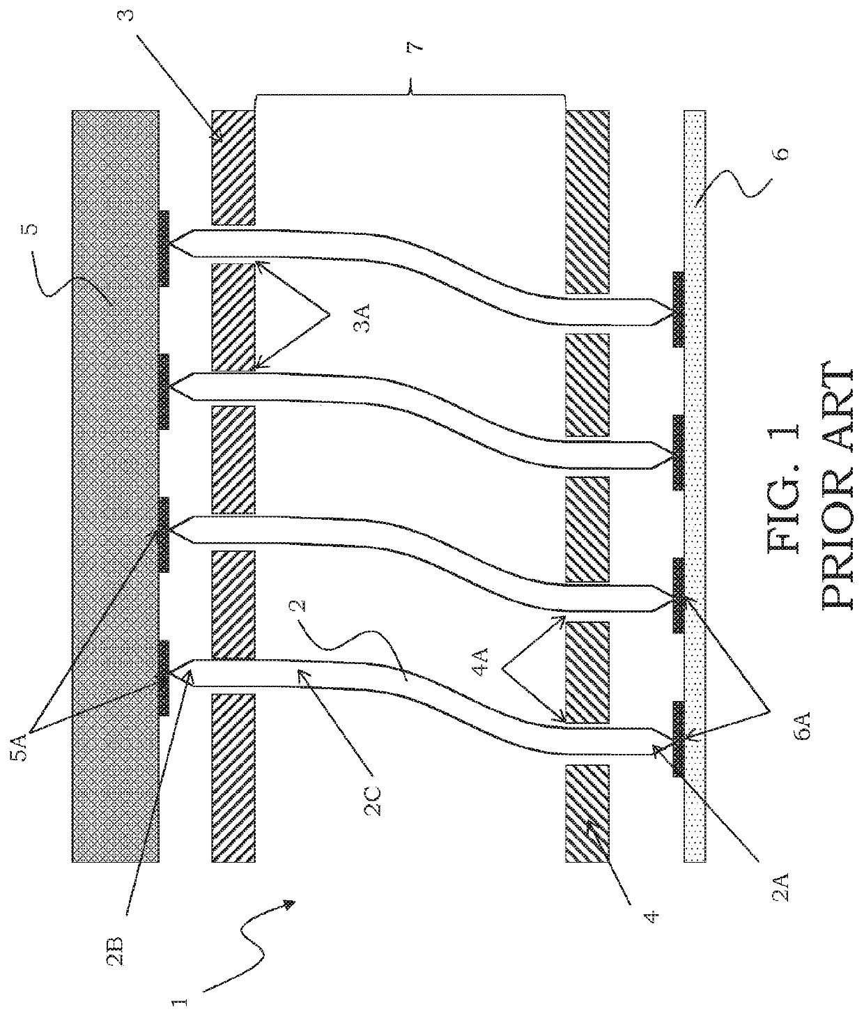
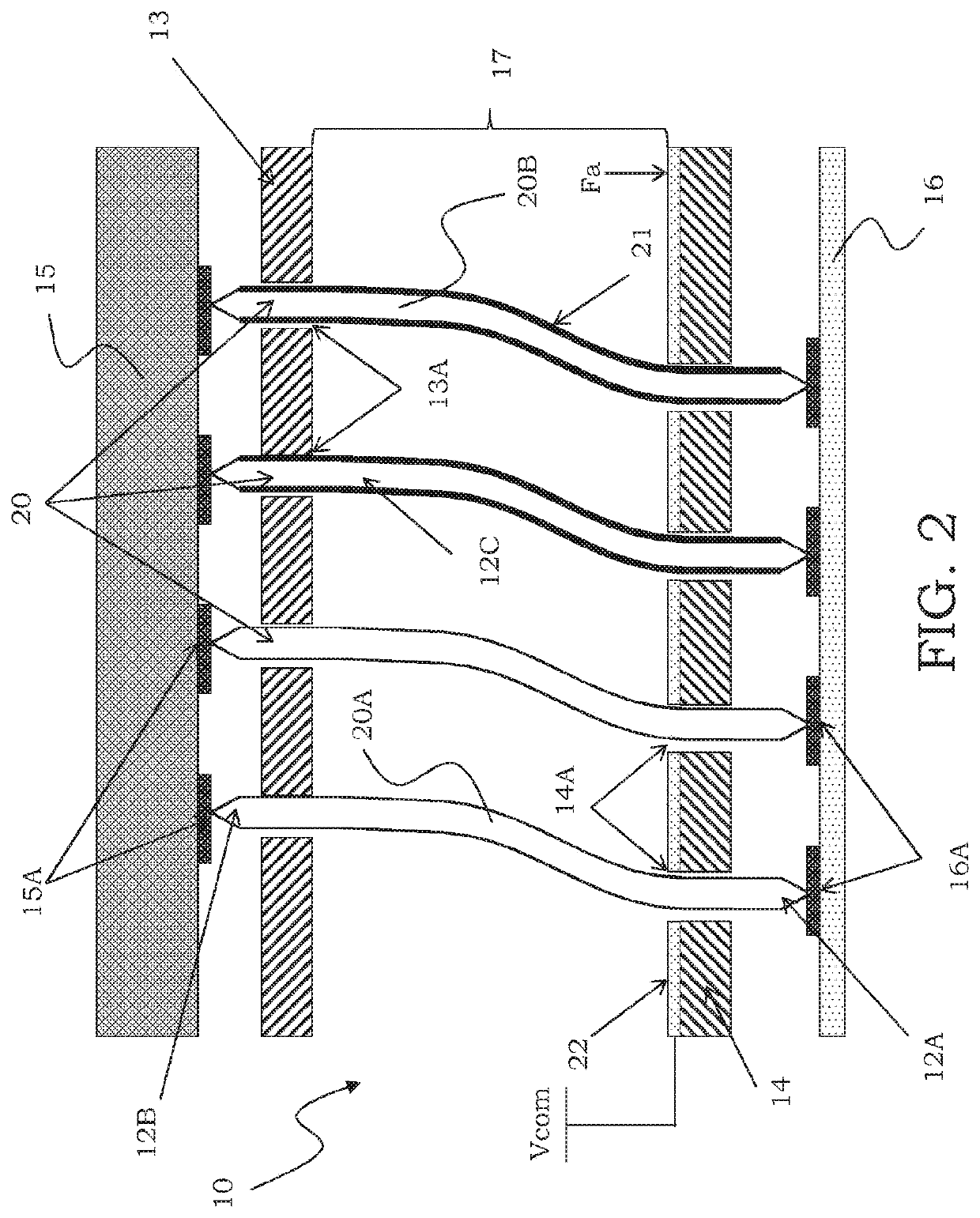
[0043]With reference to such figures, and in particular to FIG. 2, reference number 10 globally indicates a testing head provided with a plurality of contact probes for testing electronic devices, in particular integrated on wafer.

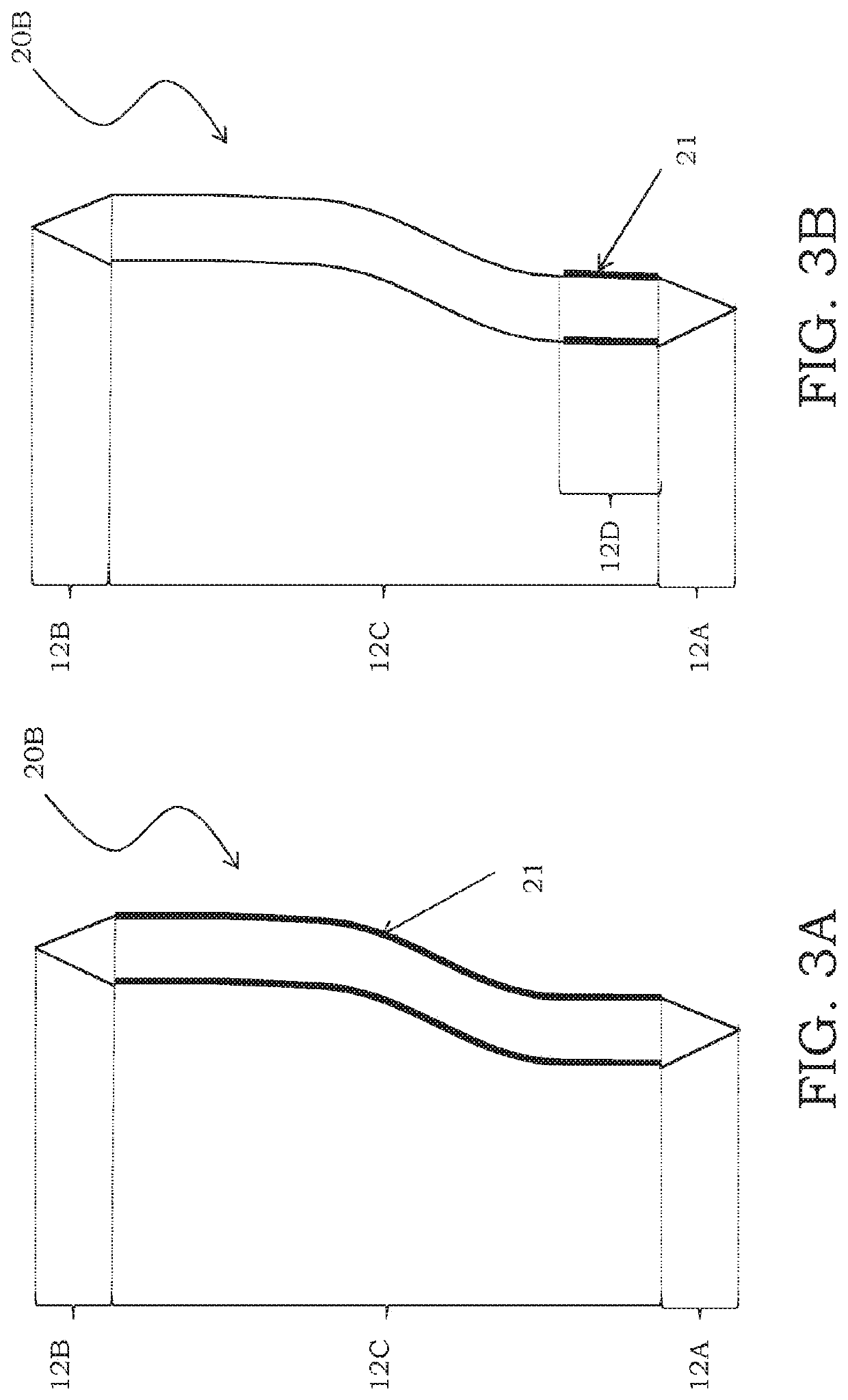
[0044]It should be noted that the figures are schematic views of the testing head according to the disclosure and are not drawn to scale, but instead they are drawn so as to enhance the important features of the disclosure. Furthermore, in the figures, the different elements are schematically shown, since their shape can vary according to the desired application. It should also be noted that in the figures identical reference numbers refer to elements identical in shape or function. Finally, the different aspects of the disclosure shown by way of example in the figures can be combined with each other and are interchangeable from one embodiment to another.

[0045]In particular, the testing head 10 is of the type with unconstrained vertical probes and comprise...


PUM


Abstract

A testing head comprises a plurality of contact probes, and a guide having a plurality of guide holes for housing the contact probes and including a conductive portion. Each contact probe includes a first end region and a second end region, and a body which extends between the first and second end regions. Suitably, the conductive portion includes a group of the guide holes and electrically connects contact probes of a first group of the contact probes. The contact probes of the first group slide in the guide holes in the conductive portion and are adapted to carry a same signal, and each contact probe of a second group of the plurality of contact probes is surrounded by an insulating coating layer that extends along the body of each contact probe of the second group, thereby insulating the contact probes of the second group from the conductive portion.

Description

BACKGROUNDTechnical Field[0001]The present disclosure refers to a testing head for testing electronic devices that are integrated on a semiconductor wafer and the following disclosure is made with reference to this field of application with the sole aim of simplifying the presentation thereof.Description of the Related Art[0002]As it is well known, a testing head is a device adapted to electrically connect a plurality of contact pads of a microstructure, in particular an electronic device that is integrated on wafer, with corresponding channels of a testing apparatus that performs the functionality testing, in particular electric, thereof, or the test, generically.[0003]The test, which is performed on integrated devices, is particularly useful in detecting and isolating defective circuits as early as in the production phase. Normally testing heads are therefore employed for the electric test of devices that are integrated on wafers before cutting or singulation and assembling them i...

Claims


Application Information

Patent Timeline
Patent Type & Authority Applications(United States)
IPC IPC(8): G01R1/073G01R1/067
CPCG01R1/06761G01R1/07371G01R1/07357G01R31/2886G01R1/06755
Inventor CRIPPA, ROBERTOMAGGIONI, FLAVIO
Owner TECHNOPROBE
Why Eureka
Try Eureka