
Package structure and method of fabricating the same

Active Publication Date: 2016-05-12
PHOENIX PIONEER TECH
View PDF3 Cites 0 Cited by
  • Summary
  • Abstract
  • Description
  • Claims
  • Application Information

AI Technical Summary

Benefits of technology

The present invention provides a package structure and method of fabrication using a single wiring layer that allows for coupling to electronic components and soldering balls, resulting in reduced signal loss and increased electronic performance. The package structure is also thinner and cheaper to fabricate due to the absence of conductive pillars or vias. Additionally, the insulative layer is made of a single material, preventing CTE mismatch and warpage.

Problems solved by technology

Therefore, the wiring arrangement, including the layout of wiring and I / O connections, is restricted.
Moreover, in a conventional QFP package structure 1, owing to the design of the leadframe, the number of leads 11, i.e., the I / O contacts are less, and it is difficult to meet the demand for high I / O connections and low profile.
However, the conventional BGA package structure 1′ still poses a problem that the signal transmission path (formed by the conductive elements 14, the wiring layers 11a and 11b, and conductive pillars 100) is too long, whereby the electrical performance of the package structure 1′ during high frequency use or high operational speed is undesirably limited.
Thus, it is difficult for the overall structure to meet the low profile requirement, and hard to reduce the fabricating cost due to the complexity of the fabricating process.
As a result, CTE mismatch would result in warpage during the fabricating process.

Method used


Image

  • Package structure and method of fabricating the same
  • Package structure and method of fabricating the same
  • Package structure and method of fabricating the same

Examples


Embodiment Construction

[0024]The present invention is described in the following with specific embodiments, so that one skilled in the pertinent art can easily understand other advantages and effects of the present invention from the disclosure of the present invention.

[0025]It should be noted that all the drawings are not intended to limit the present invention. Various modification and variations can be made without departing from the spirit of the present invention. Further, terms, such as “first”, “second”, “one” and etc., are merely for illustrative purpose and should not be construed to limit the scope of the present invention.

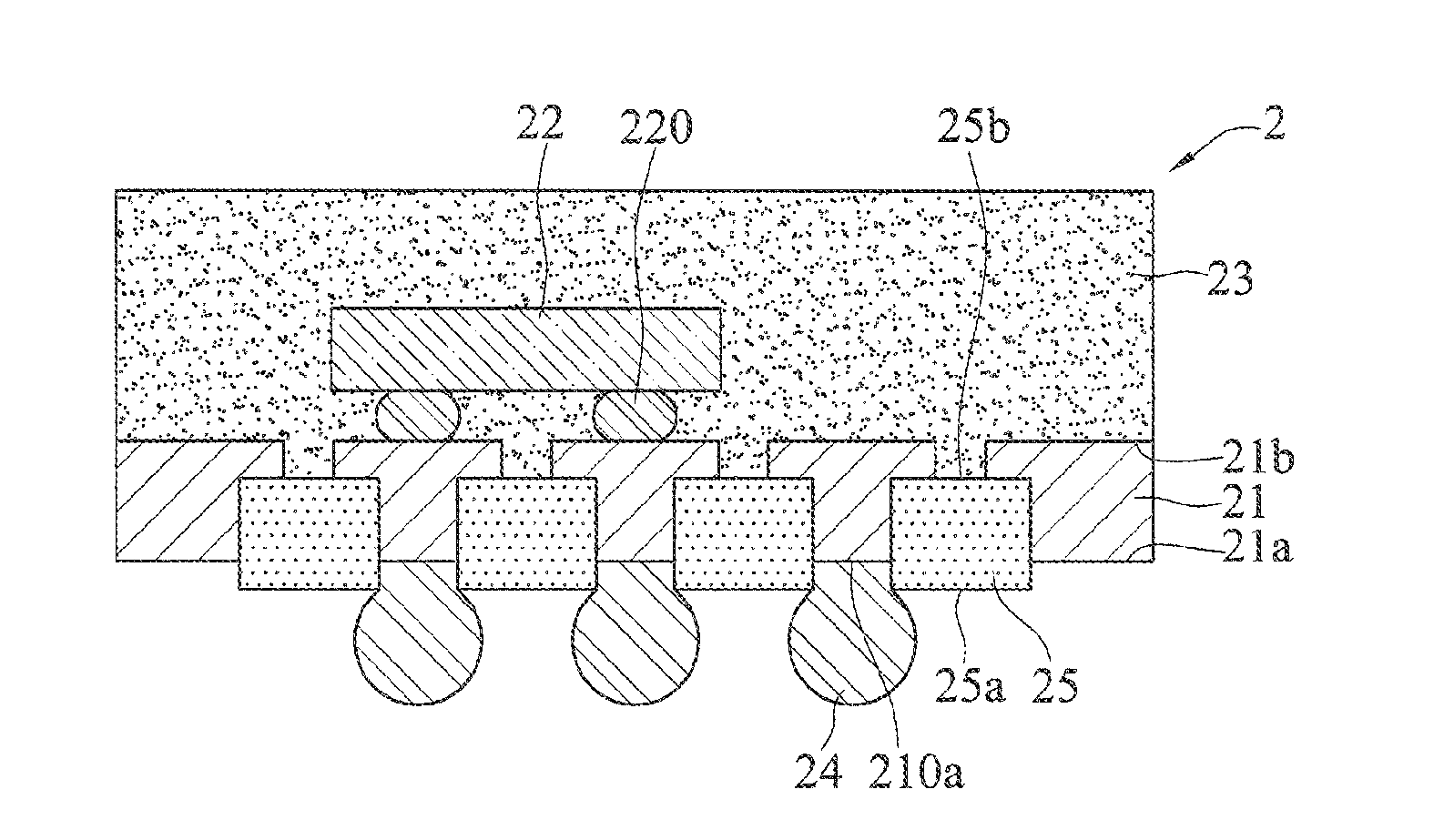
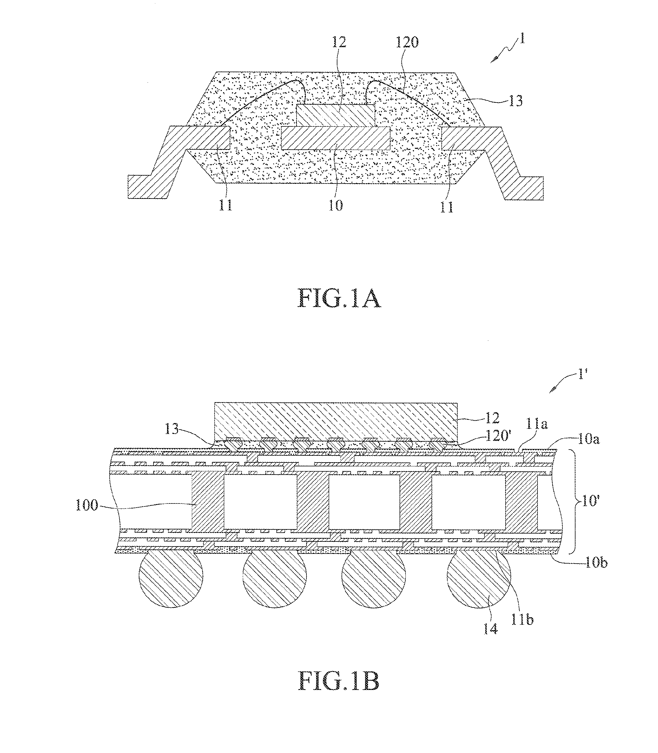
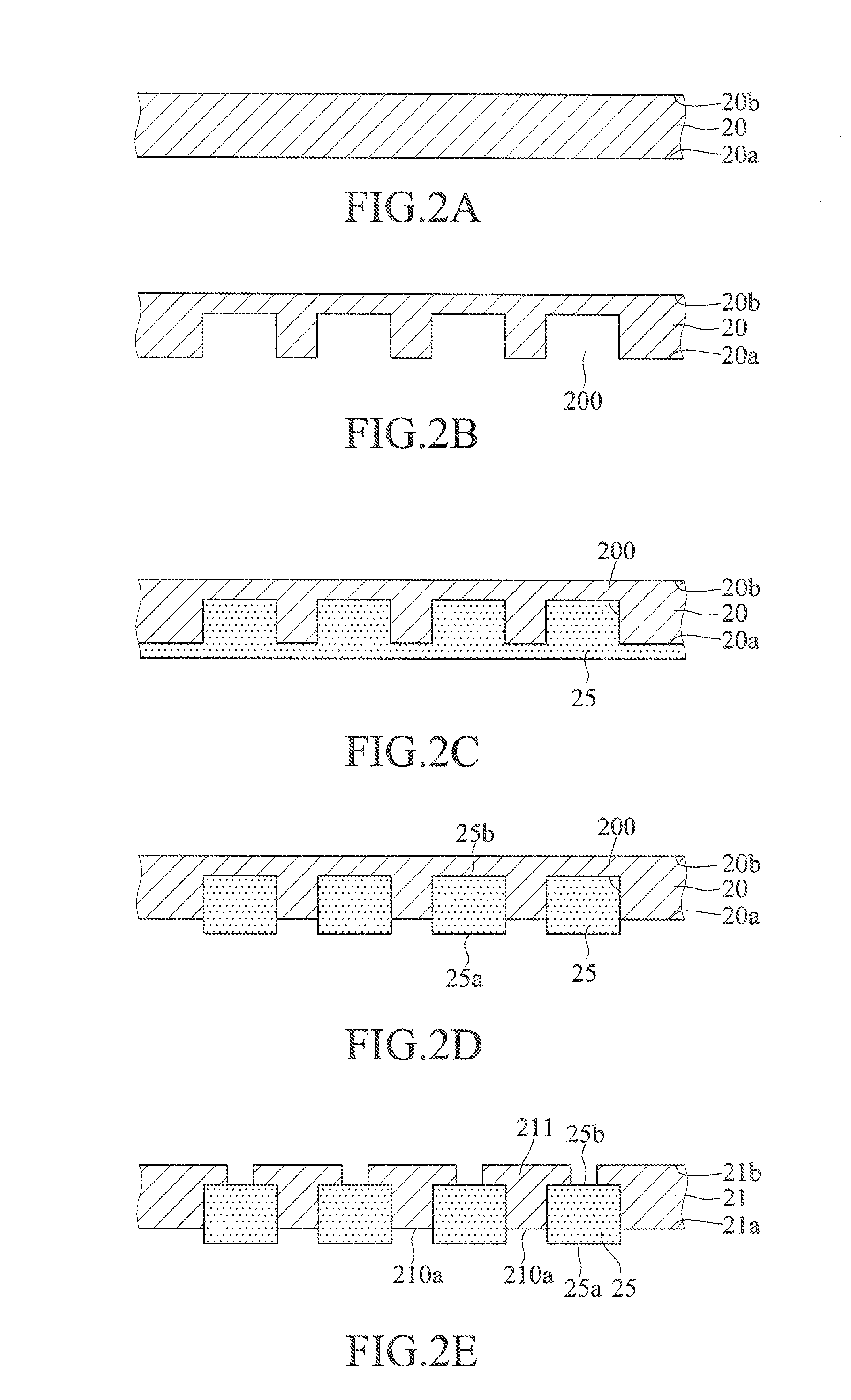
[0026]FIGS. 2A-2G are cross-sectional schematic views showing a method of fabricating a package structure 2 according to the present invention.

[0027]As shown in FIG. 2A, a conductive layer 20 having a first side 20a and an opposing second side 20b is provided.

[0028]In an embodiment, the conductive layer 20 is formed of a metal material such as copper, but is not limited theret...


PUM

PropertyMeasurementUnit
Electrical conductoraaaaaaaaaa

Abstract

A method of fabricating a package structure is provided, including forming a plurality of openings by removing a portion of the material on one side of a conductive layer, forming an insulating material as an insulating layer in the openings, removing a portion of the material on the other side of the conductive layer to serve as a wiring layer, disposing an electronic component on the wiring layer, and forming an encapsulating layer to cover the electronic component, thereby allowing the single wiring layer to be connected to the electronic component on one side and connected to solder balls on the other side thereof to shorten the signal transmission path. The present invention further provides a package structure thus fabricated.

Description

BACKGROUND OF THE INVENTION[0001]1. Field of the Invention[0002]The present invention relates to package structures, and, more particularly, to a single-layered package structure and a method of fabricating the same.[0003]2. Description of Related Art[0004]With the advancement in the technology of semiconductor package, various semiconductor devices have been developed and incorporated in smart phones, tablets, internet, and notebooks in a variety of forms, such as ball grid array (BGA), Quad-Flat Package (QFP) or Quad Flat Nonlead Package (QFN).[0005]As shown in FIG. 1A, a conventional QFP package structure 1 comprises: a carrier 10, a plurality of leads 11 surrounding the carrier 10, an electronic component 12 adhered to the carrier 10 and electrically connected to the leads 11 by a plurality of bonding wires 120, and an insulative layer 13 such as an encapsulant that encapsulates the electronic component 12, the carrier 10, the bonding wires 120 and the leads 11, wherein the lead...

Claims


Application Information

Patent Timeline
IPC IPC(8): H05K1/18H01L23/31H05K3/28H01L21/56H05K3/34H01L23/498H01L21/48
CPCH05K1/181H01L23/49816H01L23/49827H01L23/49838H01L23/3114H01L21/486H05K2203/041H01L21/56H05K3/3436H05K3/284H05K2201/095H05K2201/0183H05K2203/1377H01L21/4853H01L23/49861H01L21/4832H01L2924/181H01L2224/16225H01L2224/32225H01L2224/48091H01L2224/48247H01L2224/73204H01L2924/15311Y10T29/49146H01L23/3128H01L2924/00014H01L2924/00012H01L2924/00
Inventor HSU, SHIH-PINGLIU, CHIN-WENWU, TANG-IHU, SHU-WEI
Owner PHOENIX PIONEER TECH
Features
  • Generate Ideas
  • Intellectual Property
  • Life Sciences
  • Materials
  • Tech Scout
  • Unparalleled Data Quality
  • Higher Quality Content
  • 60% Fewer Hallucinations
Learn More