Sulfuration resistant chip resistor and method for making same

a chip resistor and sulfuration resistant technology, applied in the field of chip resistors, can solve the problems of limited platability of materials that meet such requirements (for example polymer based carbon ink), and achieve the effects of increasing the thickness of the chip resistor, good platability, and limited platability

Active Publication Date: 2011-07-19
VISHAY INTERTECHNOLOGY INC
View PDF13 Cites 11 Cited by
  • Summary
  • Abstract
  • Description
  • Claims
  • Application Information

AI Technical Summary

Benefits of technology

[0010]It is therefore a principal object, feature, aspect, or advantage of the present invention to improve over the state of the art relative to addressing the sulfuration phenomenon with chip type of resistor.
[0011]Another object, feature, or advantage of the present invention is to provide for a chip resistor which is sulfuration resistant which does not require an additional protective layer which would increase thickness of the chip resistor beyond the thickness of a standard (non-sulfuration resistant) chip resistor.
[0012]Yet another object, feature, or advantage of the present invention is a configuration or design that is applicable to all sizes of chip resistors, including the smallest ones where, for example, introduction of an additional protective layer with secure overlaps with adjacent layers would be potentially problematic.
[0013]A still further object, feature, or advantage of the present invention is to provide a chip resistor which does not have the limitations associate with the additional protective layers found in the prior art, such as being (a) conductive, (b) non-silver, (c) suitable for deposition at low temperature. Materials that meet such requirements (for example polymer based carbon ink) have limited platability.
[0014]Thus, a still further object, feature, or advantage of the present invention is to provide a sulfuration resistant chip resistor with terminals having good platability.

Problems solved by technology

Materials that meet such requirements (for example polymer based carbon ink) have limited platability.

Method used


Image

  • Sulfuration resistant chip resistor and method for making same
  • Sulfuration resistant chip resistor and method for making same
  • Sulfuration resistant chip resistor and method for making same

Examples


Embodiment Construction

[0027]For a better understanding of the invention, a specific apparatus and method of making same will now be described in detail. It is to be understood that this is but one form the invention can take. Variations obvious to those skilled in the art will be included within the invention.

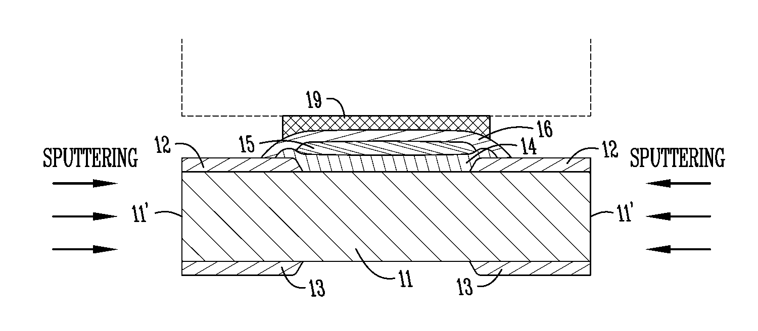
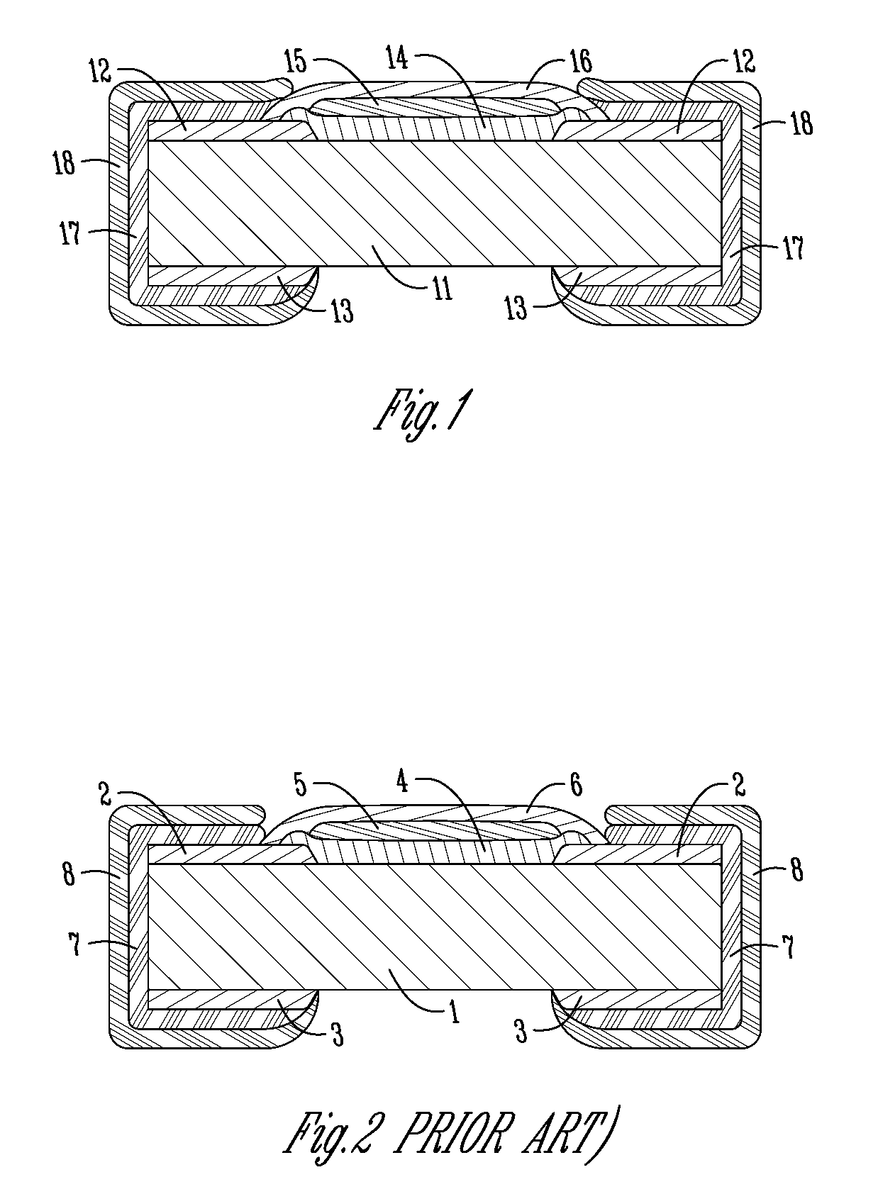
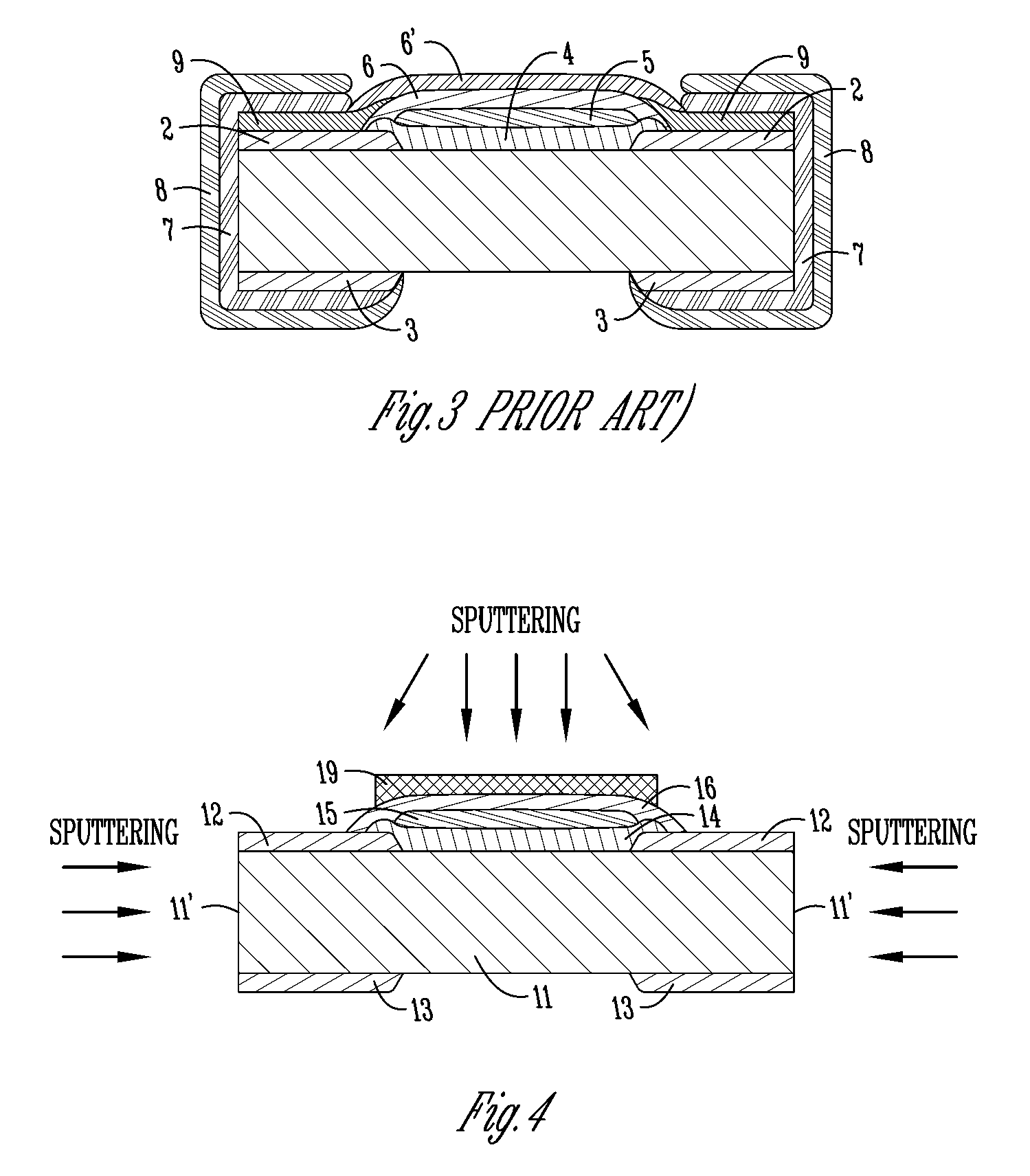
[0028]The present invention relates to a chip resistor (FIG. 1) that comprises an insulating substrate 11, top terminal electrodes 12 formed on top surface of the substrate using silver-based cermet, bottom electrodes 13, resistive element 14 that is situated between the top terminal electrodes 12 and overlaps them partially, optional internal protective coating 15 that covers resistive element 14 completely or partially, external protective coating 16 that covers completely the internal protection coating 15 and partially covers top terminal electrodes 12, plated layer of nickel 17 that covers face sides of the substrate, top 12 and bottom 13 electrodes, and overlaps partially external protective c...


PUM


Abstract

A chip resistor includes an insulating substrate 11, top terminal electrodes 12 formed on top surface of the substrate using silver-based cermet, bottom electrodes 13, resistive element 14 that is situated between the top terminal electrodes 12 and overlaps them partially, an optional internal protective coating 15 that covers resistive element 14 completely or partially, an external protective coating 16 that covers completely the internal protection coating 15 and partially covers top terminal electrodes 12, a plated layer of nickel 17 that covers face sides of the substrate, top 12 and bottom 13 electrodes, and overlaps partially external protective coating 16, finishing plated layer 18 that covers nickel layer 17. The overlap of nickel layer 17 and external protective layer 16 possesses a sealing property because of metallization of the edges of external protective layer 16 prior to the nickel plating process.

Description

CROSS-REFERENCE TO RELATED APPLICATIONS[0001]This application claims priority under 35 U.S.C. §119 to provisional application Ser. No. 60 / 892,503 filed Mar. 1, 2007, herein incorporated by reference in its entirety.BACKGROUND OF THE INVENTION[0002]The present invention relates to chip resistors, and in particular, chip resistors which are sulfuration resistant.[0003]Terminal electrodes in a majority of thick-film chip resistors and in some thin-film resistors are made of silver-based cermets. Metallic silver has several advantageous properties, including high electrical conductivity and excellent immunity to oxidizing when silver based cermets are fired in the air. Unfortunately metallic silver also has its shortcomings. Once such shortcoming is metallic silver's remarkable susceptibility to sulfur and sulfur compounds. At that, silver forms non-conductive silver sulfide resulting in open circuit in the silver-based resistor terminals. The described failure mechanism is called sulfu...

Claims


Application Information

Patent Timeline
Patent Type & Authority Patents(United States)
IPC IPC(8): H01C1/012
CPCH01C1/034H01C17/288
Inventor BELMAN, MICHAELAKHTMAN, LEONID
Owner VISHAY INTERTECHNOLOGY INC
Why Eureka
Try Eureka