Write strobe generation for a memory interface controller

a memory interface and write strobe technology, applied in digital storage, climate sustainability, instruments, etc., can solve the problems of memory errors, controller to memory interface electrical complexity, and high bandwidth and high operating frequency required to drive ddr sdram

Active Publication Date: 2011-08-02
JUMIPER NETWORKS INC
View PDF2 Cites 13 Cited by
  • Summary
  • Abstract
  • Description
  • Claims
  • Application Information

AI Technical Summary

Benefits of technology

[0005]One aspect described herein is directed to a device comprising a memory configured to store data and a memory controller connected to the memory via a number of data lines for writing a burst of data as a plurality of data signals, and a strobe line, for transmitting a strobe signal used to control writing of the data signals to the memory. The memory controller may include write data generation circuits to each transmit one of the data signals on one of the data lines, the write data generation circuits being controlled by write enable signals. The memory controller may further include a write strobe generation circuit to generate the strobe signal and the write enable signals, the strobe signal including a preamble window to signal the beginning of the data burst, a data transfer window, and a postamble window to signal the end of the data burst, the write strobe generation circuit generating the write enable signals a half memory cycle early and terminating the write enable signals a half memory cycle late with respect to the data signals generated by the write data generation circuits.

Problems solved by technology

The high bandwidth and high operating frequencies required to drive DDR SDRAM can be problematic as they can make the controller to memory interface electrically complex due to signal integrity considerations.
Static and dynamic timing variations between the strobe line and a data line can cause memory errors.
Dynamic timing variations may be caused by short or long term voltage drift and temperature changes during functional operation of the interface

Method used


Image

  • Write strobe generation for a memory interface controller
  • Write strobe generation for a memory interface controller
  • Write strobe generation for a memory interface controller

Examples


Embodiment Construction

[0016]The following detailed description of the invention refers to the accompanying drawings. The same reference numbers in different drawings may identify the same or similar elements. Also, the following detailed description does not limit the invention.

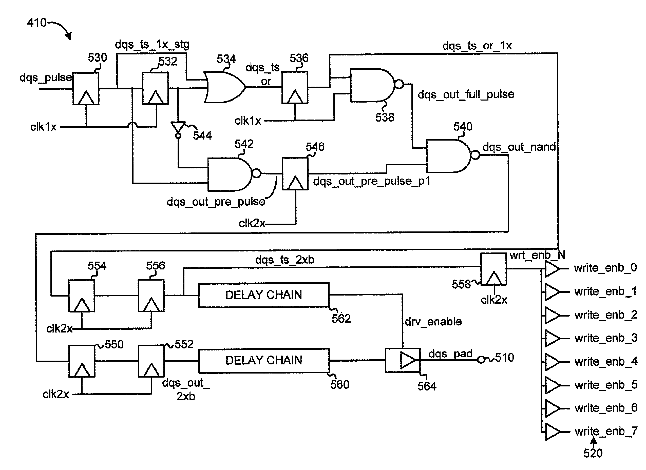
[0017]As described herein, a memory controller may include circuitry for writing data to DDR SDRAM memory. The data may be written as a burst of data in which the beginning and end of the burst are signaled by a preamble signal and a postamble signal, respectively. The memory controller may include a circuit to generate a strobe signal for write operations to the DDR SDRAM. The circuit may efficiently generate a glitch free strobe signal for a group of data lines.

Exemplary System Overview

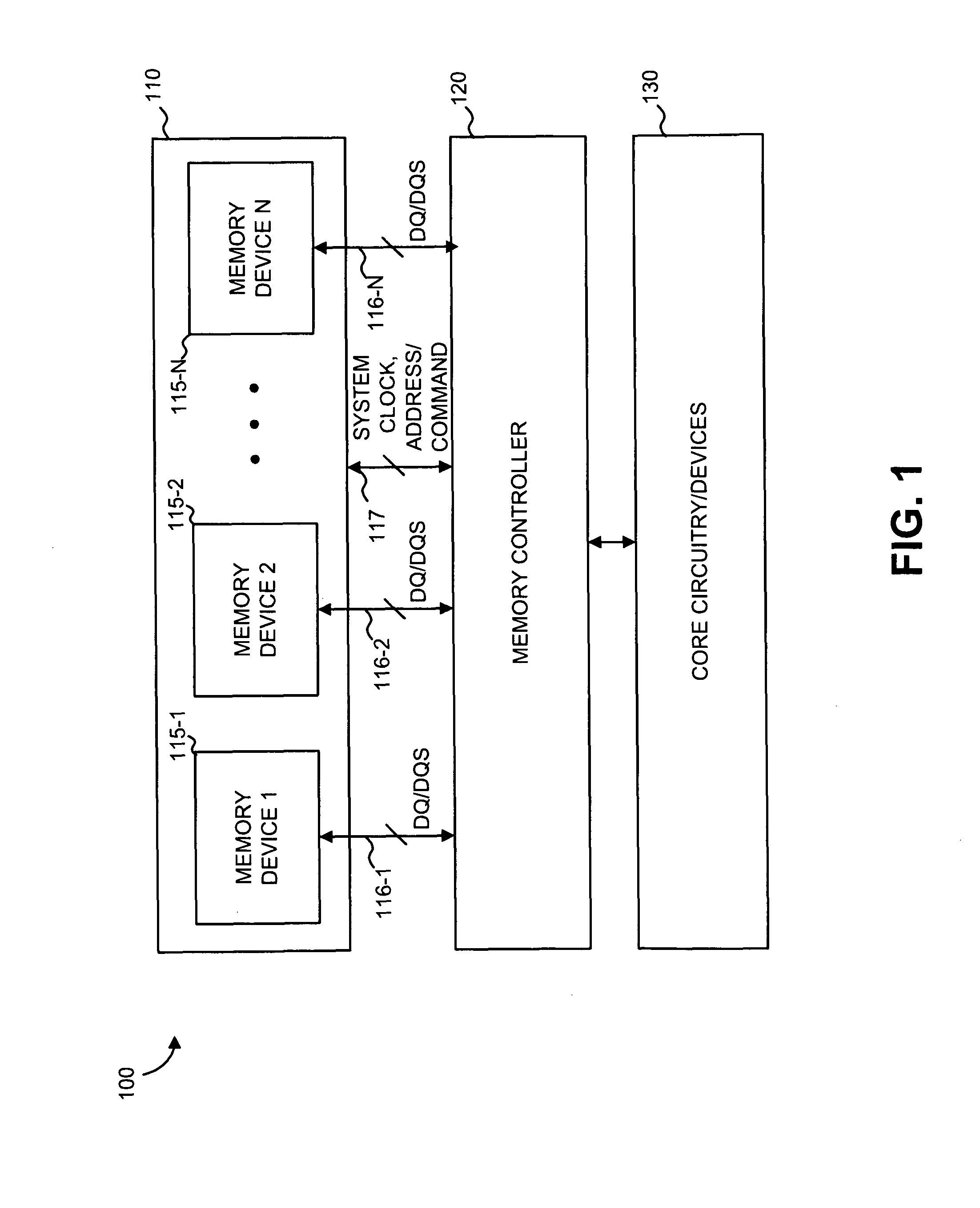
[0018]FIG. 1 is a diagram of an exemplary computing system 100 in which concepts described herein may be implemented. Computing system 100 may include a computing device that incorporates random access memory, such as DDR3 SDRAM. For instance, com...


PUM


Abstract

A memory controller includes a circuit to generate a strobe signal for write operations to a DDR SDRAM. The circuit efficiently generates a glitch free strobe signal for a group of data lines. In one implementation, the memory controller includes a write data generation circuits to each transmit a data signal to the memory on a data line, the write data generation circuits being controlled by write enable signals. A write strobe generation circuit generates the strobe signal and the write enable signals, the strobe signal including a preamble window to signal the beginning of the data burst, a data transfer window, and a postamble window to signal the end of the data burst, the write strobe generation circuit generating the write enable signals a half memory cycle early and terminating the write enable signals a half memory cycle late with respect to the data signals generated by the write data generation circuits.

Description

BACKGROUND[0001]Random access memory (RAM) is a type of storage for computing devices. RAM is typically associated with volatile memory that is implemented in integrated circuits and in which stored information is lost when power provided to the RAM is switched off.[0002]One type of RAM is known as DDR SDRAM (double-data-rate synchronous dynamic random access memory). DDR SDRAM is typically used in computing applications that require high bandwidth and low latency memory access. One version of this memory technology is known as DDR3 SDRAM, which can provide for high performance data rates, high bandwidth, high density, and low power consumption relative to earlier generations of SDRAM.[0003]The high bandwidth and high operating frequencies required to drive DDR SDRAM can be problematic as they can make the controller to memory interface electrically complex due to signal integrity considerations. A DDR3 SDRAM controller and associated memory may perform read and write operations syn...

Claims


Application Information

Patent Timeline
Patent Type & Authority Patents(United States)
IPC IPC(8): G11C7/00
CPCG06F13/1689Y02B60/1228Y02D10/00
Inventor VENKATARAMAN, SRINIVASGARAPALLY, PRAVEEN
Owner JUMIPER NETWORKS INC
Why Eureka
Try Eureka