Method for forming pattern in semiconductor device

a semiconductor device and pattern technology, applied in semiconductor devices, solid-state devices, decorative arts, etc., can solve the problems of inability to incorporate a device having a micro pattern of 40 nm or less, semiconductor devices may not include uniformly sized patterns, and disadvantages, etc., to achieve small size, improve process precision, and simplify the process

Inactive Publication Date: 2011-08-09
SK HYNIX INC
View PDF7 Cites 4 Cited by
  • Summary
  • Abstract
  • Description
  • Claims
  • Application Information

AI Technical Summary

Benefits of technology

[0016]Embodiments of the present invention are directed to provide a method for forming a pattern in a semiconductor device, which can improve process precision and simplify the process by using a positive spacer patterning technology in a region where patterns have a small size while using a negative spacer patterning technology in a region where patterns have a large size.

Problems solved by technology

Yet, it is difficult to embody a device having a micro pattern of 40 nm or less due to resolution limitations of currently developed photo-exposure apparatuses.
However, the semiconductor device may not include uniformly sized patterns.
Thus, selectively using one of the positive spacer patterning technology and the negative spacer patterning technology when forming a pattern in a semiconductor device may bring about disadvantages as well as merits.
Thus, it is difficult to form the gate patterns solely using spacers.
An additional mask process is generally required, and thus, an overlay limitation, similar to that often occurring in the double patterning technology, may be generated.
However, one of the gate patterns has to be removed because an odd number of gate patterns are formed in the cell region, causing difficulty in the process.

Method used


Image

  • Method for forming pattern in semiconductor device
  • Method for forming pattern in semiconductor device
  • Method for forming pattern in semiconductor device

Examples


Embodiment Construction

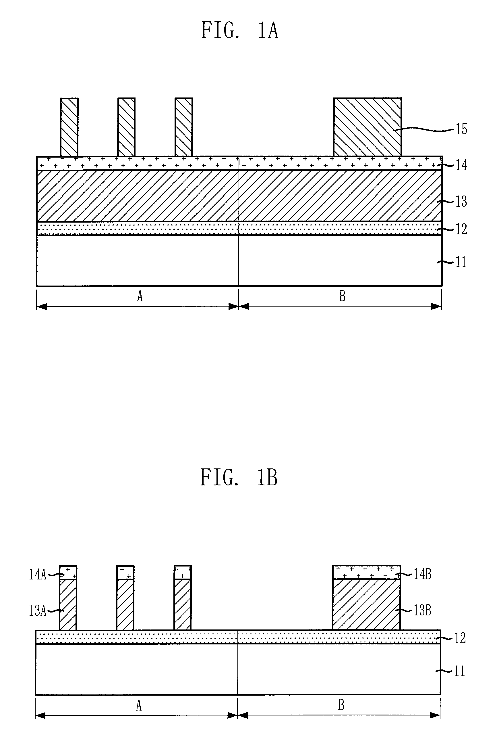
[0019]Embodiments of the present invention relate to a method for forming a pattern in a semiconductor device.

[0020]In accordance with an embodiment of the present invention, process precision is improved and the process is simplified by using a positive spacer patterning technology in a region where patterns have a small size while using a negative spacer patterning technology in a region where patterns have a large size.

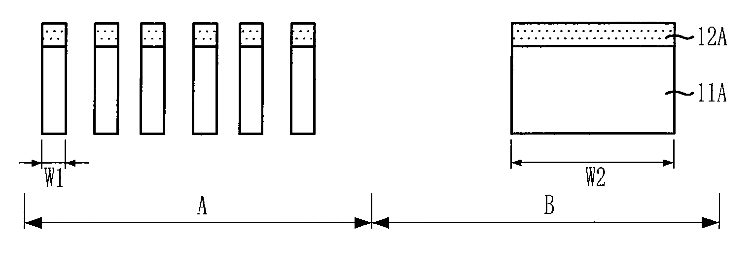
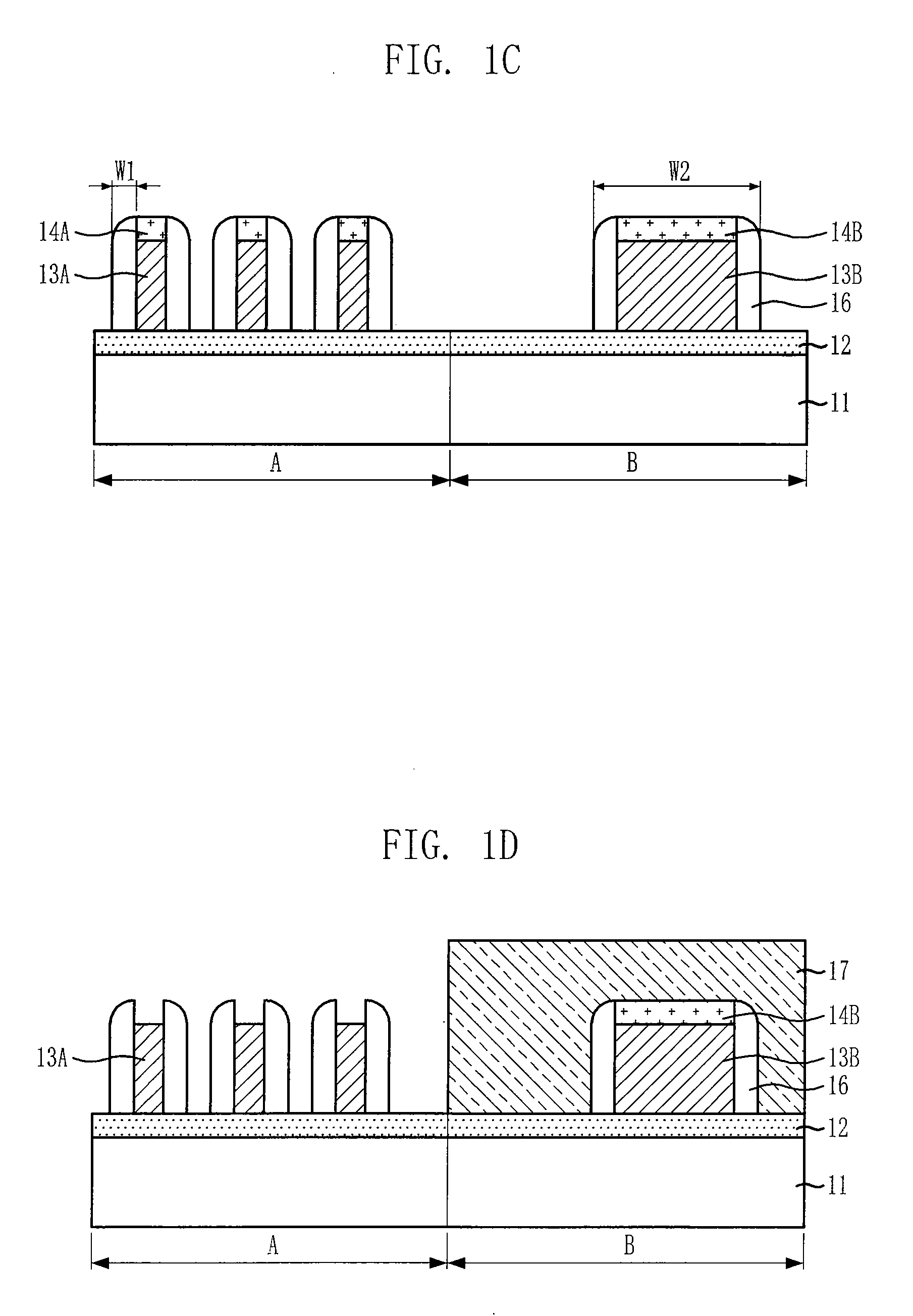
[0021]FIGS. 1A to 1H illustrate cross-sectional views of a method for forming a pattern in a semiconductor device in accordance with an embodiment of the present invention. This embodiment assumes that etch-target patterns having a first line width W1 (FIGS. 1C and 1H) are required to be formed in a first region where patterns have a small size, and other etch-target patterns having a second line width W2 (FIGS. 1C and 1H) are required to be formed in a second region where patterns have a larger size than those in the first region, wherein the second line width W2 ...


PUM

PropertyMeasurementUnit
sizeaaaaaaaaaa
widthaaaaaaaaaa
structureaaaaaaaaaa

Abstract

A method for forming a pattern in a semiconductor device includes forming an etch-target layer over a substrate, wherein the substrate includes a first region having a smaller pattern than the first region, forming a sacrificial layer and a passivation layer over the etch-target layer, etching the passivation layer and the sacrificial layer to form stack structures including a sacrificial pattern and a passivation pattern, forming spacers over sidewalls of the stack structures, forming a mask pattern covering the second region, removing a portion of the passivation pattern in the first region exposed by the mask pattern to expose a portion of the sacrificial pattern in the first region, removing the exposed portion of the sacrificial pattern in the first region, and etching the etch-target layer to form an etch-target pattern using the spacers in the first and second regions and the stack structure formed between the spacers in the second region.

Description

CROSS-REFERENCE TO RELATED APPLICATIONS[0001]The present invention claims priority of Korean patent application number 2007-0111765, filed on Nov. 2, 2007, which is incorporated by reference in its entirety.BACKGROUND OF THE INVENTION[0002]The present invention relates to a method for fabricating a semiconductor device, and more particularly, to a method for forming a pattern in a semiconductor device.[0003]As semiconductor devices have become highly integrated, pattern micronization is generally required. Yet, it is difficult to embody a device having a micro pattern of 40 nm or less due to resolution limitations of currently developed photo-exposure apparatuses.[0004]In order to overcome such limitations, a double patterning technology and a spacer patterning technology have been recently introduced. The double patterning technology includes forming a micro pattern by performing a photolithography process two times. The spacer patterning technology includes patterning using spacer...

Claims


Application Information

Patent Timeline
Patent Type & Authority Patents(United States)
IPC IPC(8): H01L21/301H01L21/461H01L21/311C03C15/00C03C25/68C23F1/00
CPCH01L21/0334H01L21/0337H01L27/105H01L27/10894H01L27/1052H10B99/00H10B12/09H01L21/308
Inventor SHIN, JONG-HANPARK, HYUNG-SOONRYU, CHEOL-HWIPARK, JUM-YONGKIM, SUNG-JUN
Owner SK HYNIX INC
Why Eureka
Try Eureka