Semiconductor device with offset stacked integrated circuits

a technology of integrated circuits and semiconductors, applied in semiconductor devices, semiconductor/solid-state device details, instruments, etc., can solve the problems of inability to supply electrical power to semiconductor chips, inability to develop and manufacture multiple types of chips to match the stacked positions, etc., and achieve the effect of improving the information transmission capability of three-dimensional coupling

Inactive Publication Date: 2011-08-09
HITACHI LTD
View PDF4 Cites 12 Cited by
  • Summary
  • Abstract
  • Description
  • Claims
  • Application Information

AI Technical Summary

Benefits of technology

[0019]In view of the above problems with the related art, the present invention has the object of providing technology for semiconductor devices that allows stacking multiple chips of the same design and also improving the information transmission capability of the three-dimensional coupling while eliminating spacers and interposers.
[0025](1) The invention achieves high-speed communication by three-dimensional coupling between semiconductor integrated circuits (semiconductor chips), communication by physical wiring between the semiconductor integrated circuit and outside the package; and supply of power to the semiconductor integrated circuit.(2) The invention reduces the costs required for developing semiconductor chips to a minimum.

Problems solved by technology

However a study of the above semiconductor devices of the related art by the present inventors revealed the following problems.
Supplying electrical power to the semiconductor chips for example is impossible when using either of the inductive or capacitive type coupling methods.
Also, when forming a SiP from multiple stacked semiconductor chips with the same function, developing and manufacturing multiple types of chips to match the stacked positions is not desirable.

Method used


Image

  • Semiconductor device with offset stacked integrated circuits
  • Semiconductor device with offset stacked integrated circuits
  • Semiconductor device with offset stacked integrated circuits

Examples


first embodiment

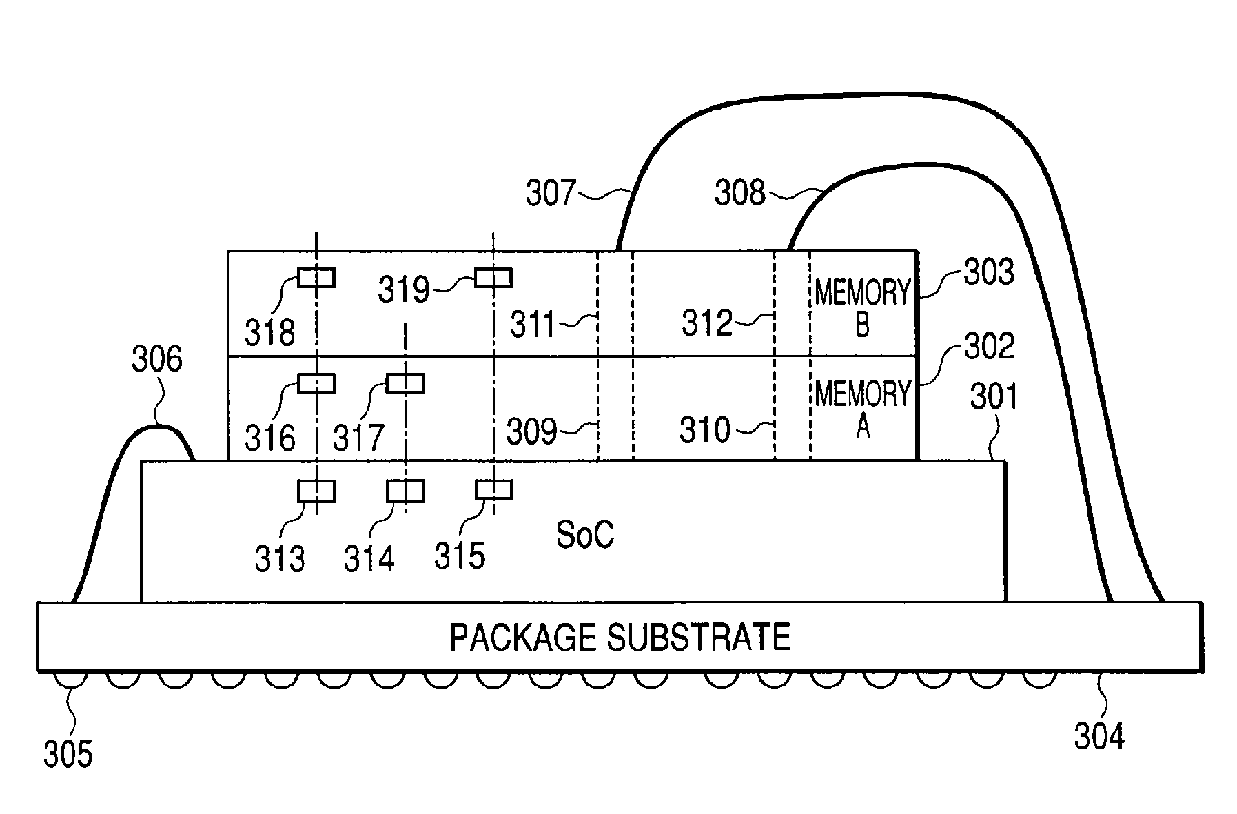
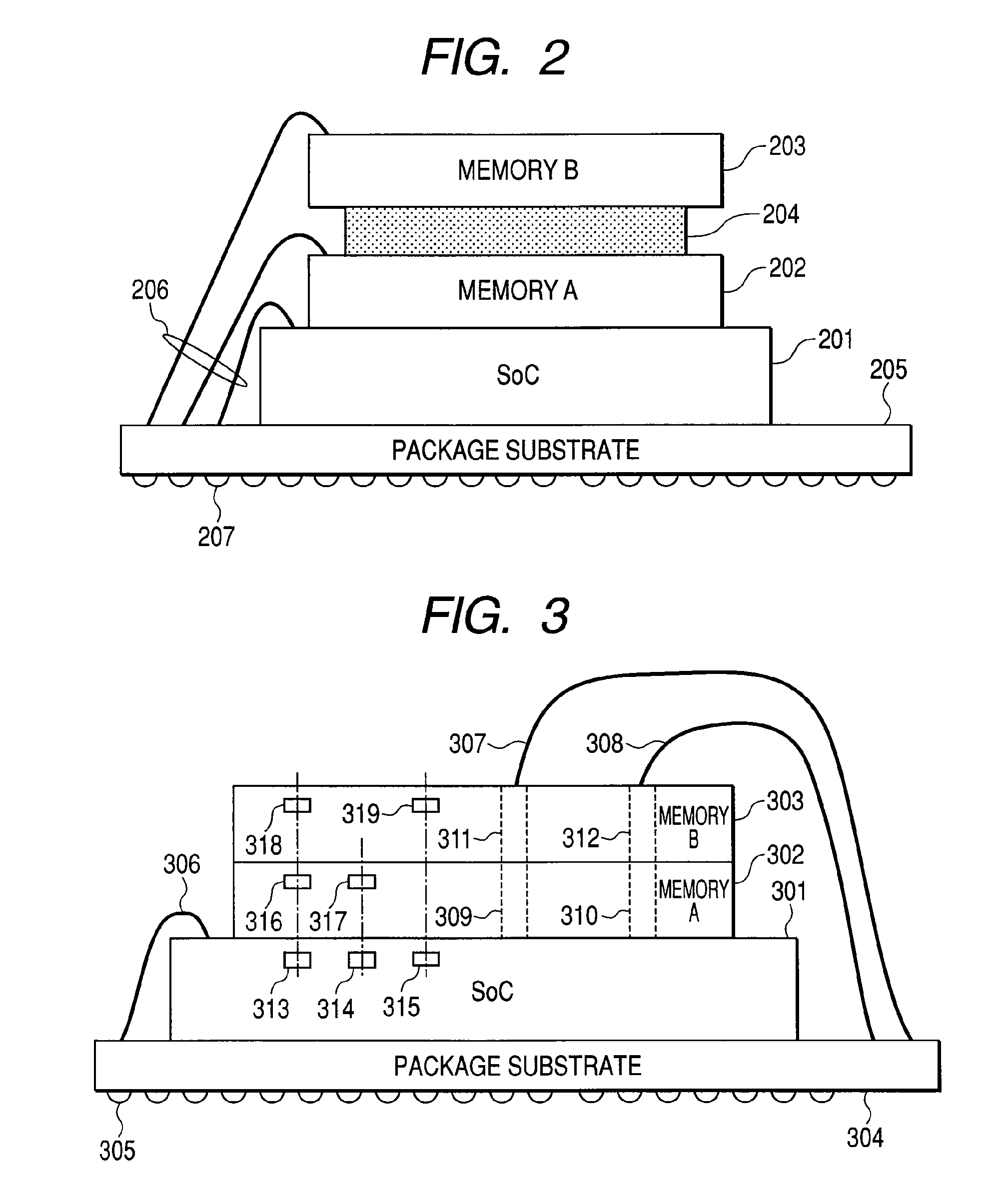
[0061]The first embodiment of this invention is stacked semiconductor integrated circuits contained in the SiP with the terminals set upwards and connected by bonding wire.

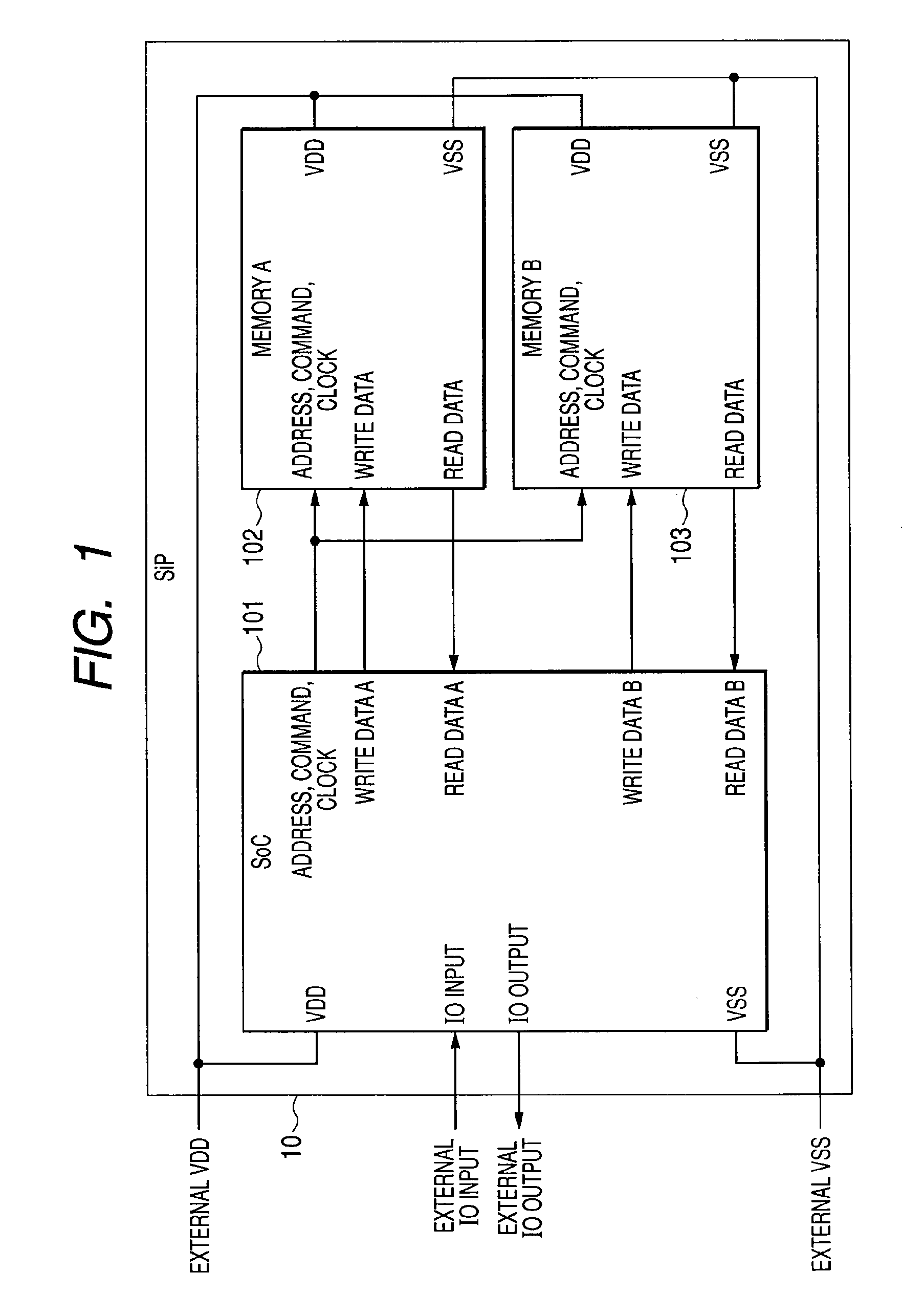
[0062]FIG. 1 is a block diagram showing the structure of the semiconductor device of the first embodiment of this invention. FIG. 1 is a logical block diagram showing the related functional connections for the System In Package (Hereafter, called SIP.) of the first embodiment of this invention.

[0063]The SiP 10 contains a SoC101, a memory A102, and a memory B103 as well as a function for communicating outside the SiP10. The SoC101 implements the applicable communication function by loading the program stored in the memory A102 and memory B103. The SoC101 also contains a function for writing on the memory A102 and the memory B103.

[0064]The SoC101 as well as memory A102 and memory B103 are semiconductor integrated circuits made for example from single crystal silicon and including CMOS (complementary MOS transistors)...

second embodiment

[0123]The second embodiment of this invention stacks the semiconductor integrated circuit face-down in the SiP. The physical structure of the SiP of the second embodiment is described next. The logical structure of the SiP of the second embodiment is identical to the logical structure of the SiP of the first embodiment.

[0124]FIG. 11 is a drawing of the semiconductor integrated circuit mounted in the SiP of the second embodiment of this invention as seen from a horizontal view.

[0125]The SoC1101, the memory A1102 and the memory B1103 are all mounted face-down in the SiP20.

[0126]The structure of the SiP20 is described first.

[0127]The SiP20 contains an SoC1101, the memory A1102 and the memory B1103, the package substrate 1104, the external terminal 1105, and the micro-bumps 1106-1108.

[0128]The SoC1101, the memory A1102, and the memory B1103 correspond to the respective SoC1101, memory A102, and memory B103 in FIG. 1.

[0129]The memory A1102 of the second embodiment is identical to the mem...

third embodiment

[0146]In the first and second embodiments, three-dimensional communication was directly performed between the SoC and memory A, and also between the SoC and memory B. However the inductive coupling coefficient is inversely proportional to the square of the distance between the coils so three-dimensional coupling to couple the memory B to the SoC requires installing a large coil because of the long distance between the chips. This large coil reduces the number of installable coils, and does not allow raising the data transfer rate.

[0147]The third embodiment described next is a method for communicating with a small coil by utilizing a chip with a signal relay function positioned in the intermediate layer.

[0148]The SiP function of the third embodiment is identical to that of the first embodiment.

[0149]FIG. 14 is a drawing showing a horizontal view of the semiconductor integrated circuit mounted on the SiP210 in the third embodiment of this invention.

[0150]The SoC2101, the memory A2102,...


PUM


Abstract

A semiconductor device where multiple chips of identical design can be stacked, and the spacer and interposer eliminated, to improve three-dimensional coupling information transmission capability. A first semiconductor circuit including a three-dimensional coupling circuit (three-dimensional coupling transmission terminal group and three-dimensional coupling receiver terminal group); and a second semiconductor integrated circuit including a three-dimensional coupling circuit and feed-through electrode (power supply via hole and ground via hole); and a third semiconductor integrated circuit including a three-dimensional coupling circuit and feed-through electrode are stacked on the package substrate.

Description

CLAIM OF PRIORITY[0001]The present application claims priority from Japanese patent application JP 2007-185425 filed on Jul. 17, 2007, the content of which is hereby incorporated by reference into this application.FIELD OF THE INVENTION[0002]The present invention relates to a semiconductor device, and relates in particular to technology effective for use with SiP (System in Package) made up of stacked semiconductor integrated circuits and semiconductor integrated circuits used in microprocessors, etc.BACKGROUND OF THE INVENTION[0003]The technology studied by the inventors may include the following technology for semiconductors.[0004]Along with the increasing device miniaturization achieved by semiconductor manufacturing technology, the problem of inadequate I / O capability on semiconductor chips is becoming more and more serious.[0005]This problem of inadequate I / O capability is due to an increasing number of circuits as the semiconductor chips become smaller. Moreover as the operati...

Claims


Application Information

Patent Timeline
Patent Type & Authority Patents(United States)
IPC IPC(8): H01L23/02H01L27/00
CPCH01L23/48H01L25/0657H01L24/06H01L25/18H01L2924/1305H01L2224/0401H01L2224/48091H01L2224/48227H01L2225/0651H01L2225/06527H01L2225/06541H01L2225/06562H01L2225/06575H01L2924/01004H01L2924/01014H01L2924/01033H01L2924/01082H01L2924/15311H01L2924/19041H01L2924/30107H01L2924/13091H01L2224/73265H01L2224/32225H01L2224/32145H01L2224/16225H01L2924/01075H01L2924/01055H01L2924/01047H01L2924/01006H01L2924/01005H01L24/48H01L2924/00014H01L2924/00012H01L2924/00H01L24/73H01L2924/181H01L2924/14H01L2224/45099H01L2224/45015H01L2924/207H01L23/12H01L23/045
Inventor NONOMURA, ITARUOSADA, KENICHISAEN, MAKOTO
Owner HITACHI LTD
Why Eureka
Try Eureka