Nanoparticle cap layer

a technology of nanoparticles and caps, applied in the direction of electrical equipment, semiconductor devices, semiconductor/solid-state device details, etc., can solve the problems of small nanoparticles melted and wet copper surfaces, and achieve the effect of effectively “wet” nanoparticles and high surface energy

Active Publication Date: 2011-08-09
NOVELLUS SYSTEMS
View PDF21 Cites 17 Cited by
  • Summary
  • Abstract
  • Description
  • Claims
  • Application Information

AI Technical Summary

Benefits of technology

[0013]The nanoparticles attached to the surface are then optionally annealed to form a cap layer. The annealing operation may drive copper diffusion into the nanoparticle layers and effectively “wet” the nanoparticles. The result is a metal cap layer of nanoparticles intermixed with metal from the selected surface (e.g., copper) at about 20 atomic % or greater of the substrate metal. The resulting metal cap layer may have an effective thickness of about 0.3 to 10 nm, depending on how many layers are deposited, the filling ratio, anneal conditions, etc. In certain embodiments, the nanoparticles might also wet the selected surface at temperatures much less than the melting point of the nanoparticles material due to the high surface energy of the nanoparticles relative to bulk.

Problems solved by technology

In another case the small nanoparticles may melt and wet the copper surface due to the large surface energy of the nanoparticles.

Method used


Image

  • Nanoparticle cap layer
  • Nanoparticle cap layer
  • Nanoparticle cap layer

Examples


Embodiment Construction

Introduction

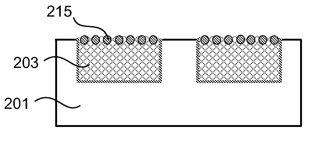
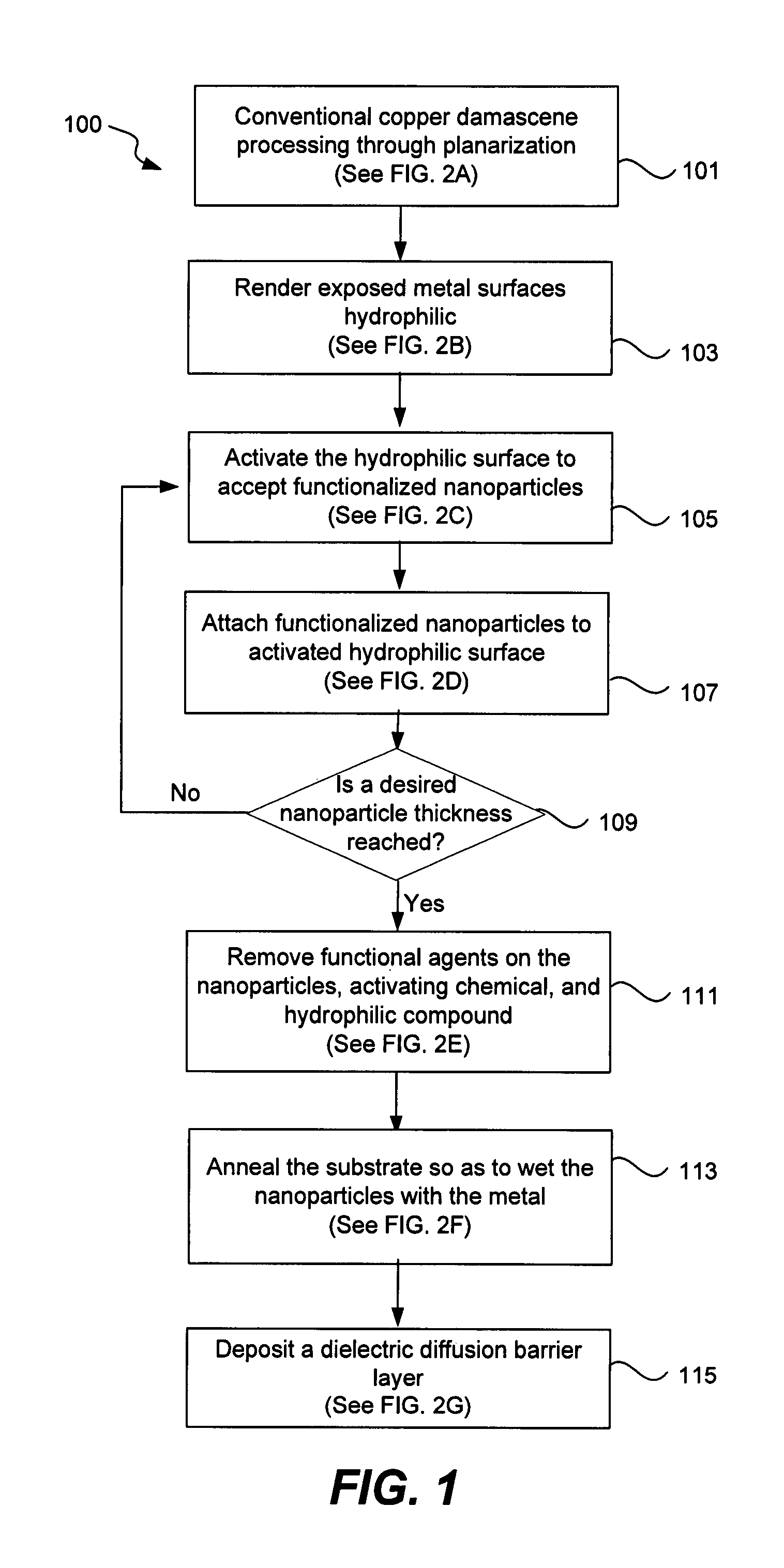
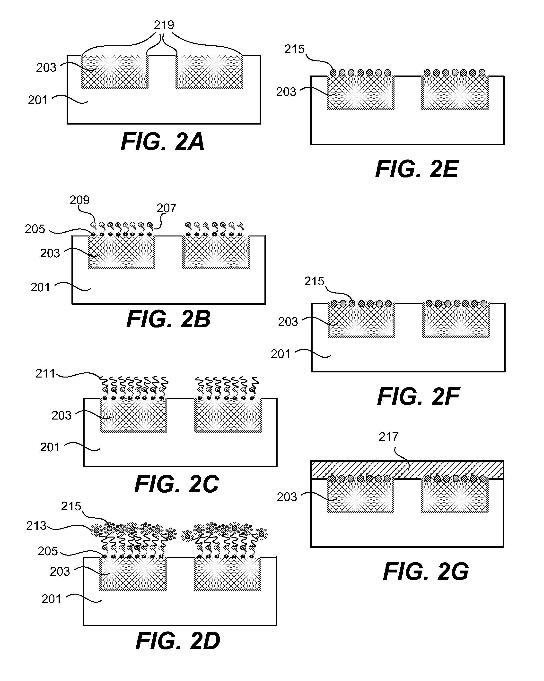
[0024]Embodiments of the present invention are described herein in the context of a metal cap layer on top of copper lines. Those of ordinary skill in the art will realize that the following detailed description of the present invention is illustrative only and is not intended to be in any way limiting. Other embodiments of the present invention will readily suggest themselves to such skilled persons having the benefit of this disclosure. For example, although capping of copper lines is discussed, the selective nanoparticle deposition of a metal cap layer is applicable on other types of metal features (e.g., aluminum interconnects). Further, selective nanoparticle deposition may be appropriate on non-metal surfaces as well.

[0025]Reference will be made in detail to implementations of the present invention as illustrated in the accompanying drawings. The same reference indicators will be used throughout the drawings and the following detailed description to refer to the sa...


PUM

PropertyMeasurementUnit
sizeaaaaaaaaaa
thickaaaaaaaaaa
diametersaaaaaaaaaa

Abstract

Functionalized nanoparticles are deposited on metal lines inlaid in dielectric to form a metal cap layer that reduces electromigration in the metal line. The functionalized nanoparticles are deposited onto activated metal surfaces, then sintered and annealed to remove the functional agents leaving behind a continuous capping layer. The resulting cap layer is about 1 to 10 nm thick with 30-100% atomic of the nanoparticle material. Various semiconductor processing tools may be adapted for this deposition process without adding footprint in the semiconductor fabrication plant.

Description

FIELD OF INVENTION[0001]The present invention pertains to methods and apparatus used in device fabrication processes, and more particularly to methods and apparatus used to deposit material onto a semiconductor substrate. The methods and apparatus are particularly useful for forming a metal cap layer on top of embedded metal lines.BACKGROUND OF THE INVENTION[0002]Electromigration reliability is a serious concern for interconnects. Electromigration is an atomic-scale phenomenon in which the moving electrons that constitute electric-current collide with the metal-atoms of an interconnect line and push them in the direction of the current flow. Given enough collisions over time, a significant migration of the metal atoms will occur. This transport of material can lead to formation of voids and consequent increase in resistance, and ultimately lead to the electrical failure of the interconnect by breaking the line. Electromigration defects occur principally at interfaces between metal l...

Claims


Application Information

Patent Timeline
Patent Type & Authority Patents(United States)
IPC IPC(8): H01L23/48
CPCH01L21/288H01L21/67161H01L21/67196H01L21/76834H01L21/76849
Inventor ALERS, GLENNHAVEMANN, ROBERT H.
Owner NOVELLUS SYSTEMS
Why Eureka
Try Eureka