Solid-state imaging device

a solid-state imaging and imaging device technology, applied in the direction of color television, television system, radio control device, etc., can solve the problems of difficult fabrication of structures, inability to avoid incident light passing through thicker multi-level metallization structures, etc., to achieve the suppression of incident light attenuation and scattering, and the effect of more highly integrated circuits

Active Publication Date: 2011-09-06
SOCIONEXT INC
View PDF14 Cites 2 Cited by
  • Summary
  • Abstract
  • Description
  • Claims
  • Application Information

AI Technical Summary

Benefits of technology

[0011]Moreover, if image sensor chip for camera modules is disigned as a large-scale integrated circuit, it is impossible to avoid having the incident light pass through the thicker multilevel metallization structure (e.g., a five-layer structure) of the peripheral circuitry. Accordingly, there has existed a desire for a multilevel metallization structure which is simple and which minimizing the scattering and attenuation of incident light to the pixels.
[0012]It is therefore an object of the invention to provide a solid-state imaging device having the multilevel metallization structure needed for larger-scale integration and a smaller chip size, and also having a structure capable of effectively suppressing the scattering and attenuation of incident light to the pixels.
[0014]According to this first aspect of the invention, over the peripheral circuitry portion, the first multilevel metallization structure enables highly integrated circuits to be provided in a small surface area. At the same time, over the pixel array portion having a plurality of pixels, the formation of a second multilevel metallization structure which is thinner than the first multilevel metallization structure enables the scattering and attenuation of incident light to the pixels to be suppressed. Moreover, by giving the multilevel metallization structure over the pixel array portion a uniformly thin structure, the fabrication process can be simplified.
[0015]In a preferred embodiment of the above first aspect of the invention, the first multilevel metallization structure over the peripheral circuitry portion and the second multilevel metallization structure over the pixel array portion form a single trench structure over the pixel array, the trench structure has a protrusion in at least one corner thereof. The solid-state imaging device according to this embodiment also has a color filter film formed on a bottom of the trench structure by spin coating and has a microlens over each pixel. The resin material applied during spin coating to form the color filter film or microlenses is pushed against the protrusion, enabling the formation of a uniform film on the bottom of the trench structure.
[0020]In the solid-state imaging device of the invention, a thicker multilevel metallization structure is provided over the peripheral circuitry portion, enabling more highly integrated circuits and a smaller chip size to be achieved. At the same time, a thinner multilevel metallization structure is provided over the pixel array, enabling the attenuation and scattering of incident light to be suppressed.

Problems solved by technology

However, such structures are quite difficult to fabricate.
Moreover, if image sensor chip for camera modules is disigned as a large-scale integrated circuit, it is impossible to avoid having the incident light pass through the thicker multilevel metallization structure (e.g., a five-layer structure) of the peripheral circuitry.

Method used


Image

  • Solid-state imaging device
  • Solid-state imaging device
  • Solid-state imaging device

Examples


first embodiment

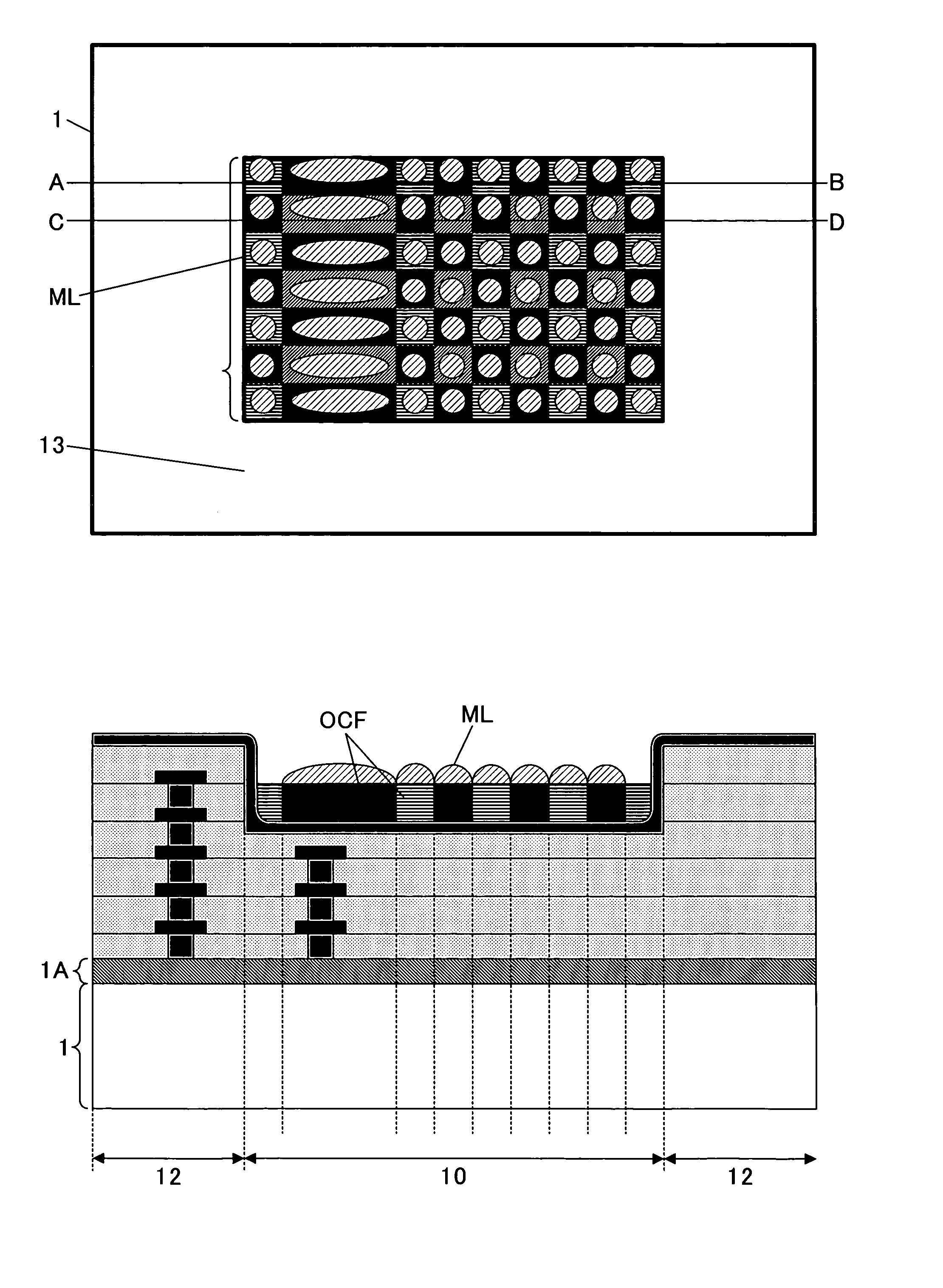
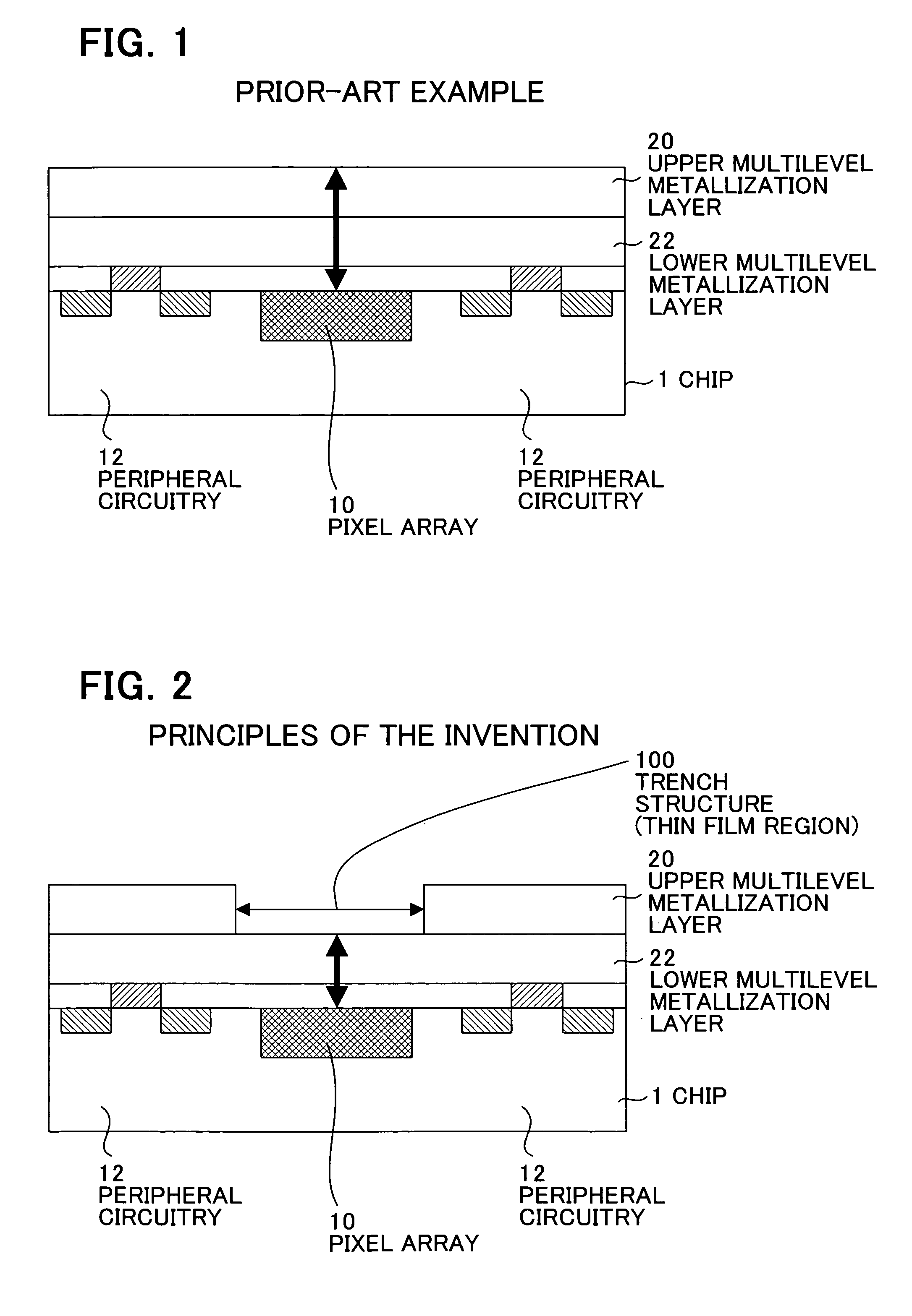
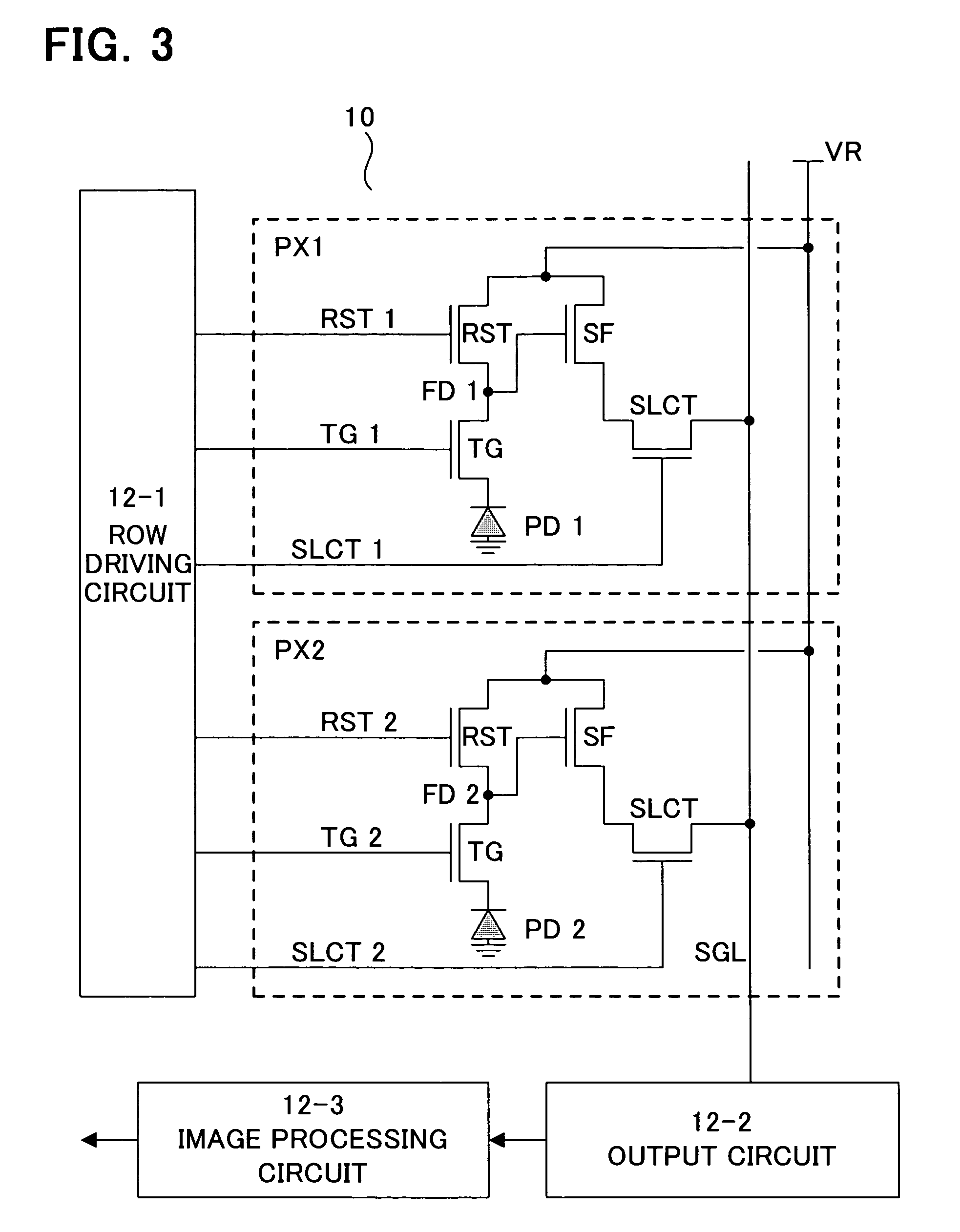
[0039]FIG. 4 is a diagram of an image sensor according to the invention. FIG. 4A is a cross-sectional view of an image sensor chip 1 housed in a package 2, and FIG. 4B is a plan view of the chip 1. The chip 1, which is an image sensor, is contained within the package 2, and a condensing lens 4 is provided at the top of the package 2. The chip 1 has a pixel array portion 10 at the center, and peripheral circuitry portion 12. Here, for the sake of convenience, pixel array portion 10 and periphery circuitry portion 12 each include both circuit elements within the chip and a lower multilevel metallization structure (represented by the reference symbol 22 in FIG. 2). In addition, an upper multilevel metallization structure 20 is provided above the peripheral circuitry portion 12.

[0040]The pixel array portion 10 has a black pixel region 13 at the periphery and a light-receiving pixel region 11 at the center. The black pixel region 13 is composed of a barrier film or the like so as not to ...

second embodiment

[0042]FIG. 5 is a diagram of an image sensor according to the invention. As in FIG. 4, FIG. 5A is a cross-sectional view of an image sensor chip 1 housed in a package 2, and FIG. 5B is a plan view of the chip 1. The pixel array portion 10 and the peripheral circuitry portion 12 on the chip 1 are the same as in FIG. 4.

[0043]In this embodiment, the light-collecting convex lens 4 is large and exterior light is collected through this to the light-receiving pixel region 11. In addition, the size of the trench structure 100 has been made wider than the light-receiving pixel region 11 so as to keep the incident light from being blocked by the upper multilevel metallization layer 20. Here too, the upper multilevel metallization layer 20 is formed over both the peripheral circuitry portion 12 and part of the black pixel region 13, thus enabling the surface area of the power distribution plane formed on the multilevel metallization layer 20 to be increased.

third embodiment

[0044]FIG. 6 is a diagram of an image sensor according to the invention. As in FIG. 5, FIG. 6A is a cross-sectional view of an image sensor chip 1 housed in a package 2, and FIG. 6B is a plan view of the chip 1. FIG. 6A is similar to FIG. 5A.

[0045]In this embodiment, protrusions 100A are formed at the four corners of the trench structure 100 on the pixel array 10. In other respects, this embodiment is identical to the second embodiment described above. These protrusions 100A are provided so as to enable a layer of liquid material to form to a uniform film thickness at the bottom of the trench structure 100 when an optical color filter, microlens or photoreceptor resistor is produced by spin coating a layer of liquid material onto the trench structure 100.

[0046]FIG. 7 illustrates a spin coating method used to form a layer of liquid material on the trench structure in the third embodiment of the invention. In this spin coating method, the semiconductor wafer is mounted on a spinner an...


PUM


Abstract

A solid-state imaging device has a substrate in which are formed a pixel array portion having a plurality of pixels, and a peripheral circuitry portion. The device is characterized in that a first multilevel metallization structure is formed over the peripheral circuitry portion, and a second multilevel metallization structure thinner than the first multilevel metallization structure is formed over the pixel array portion.

Description

CROSS-REFERENCE TO RELATED APPLICATIONS[0001]This application is based upon and claims the benefit of priority from the prior Japanese Patent Application No. 2005-89268, filed on Mar. 25, 2005, the entire contents of which are incorporated herein by reference.BACKGROUND OF THE INVENTION[0002]1. Field of the Invention[0003]The present invention relates to a solid-state imaging device, and more particularly to a solid-state imaging device based on CMOS technology.[0004]2. Description of the Related Art[0005]The CMOS-based solid-state imaging device, generally an active pixel sensor or a CMOS image sensor, has within each pixel of a pixel array a photoelectric convertor and transistors which reset and amplify the convertor, and has, in peripheral circuitry, drive circuits which drive the individual pixels and also output circuits and image processing circuits which amplify electrical signals output from the individual pixels and carry out image processing. It is anticipated that such C...

Claims


Application Information

Patent Timeline
Patent Type & Authority Patents(United States)
IPC IPC(8): H01L31/062H01L27/14H01L27/146H04N5/335H04N5/369
CPCH01L27/14609H01L27/14629H01L27/14643H01L27/14636H01L27/14621H01L27/14625H01L27/14685H01L27/146
Inventor KOBAYASHI, HIROSHIYAMAMOTO, KATSUYOSHIINOUE, TADAOMIZUGUCHI, TOSHITAKA
Owner SOCIONEXT INC
Why Eureka
Try Eureka