Source follower with gain compensation, and circuits and methods for source follower gain error compensation

a source follower and gain compensation technology, applied in the field of source follower circuits, can solve the problems of non-ideality of a typical source follower circuit, gain is still limited by the source-drain output resistance of the input transistor, further gain errors and non-linearities, etc., to reduce the non-linearity of a source follower and improve gain and frequency response.

Inactive Publication Date: 2011-09-20
MARVELL INT LTD
View PDF1 Cites 15 Cited by
  • Summary
  • Abstract
  • Description
  • Claims
  • Application Information

AI Technical Summary

Benefits of technology

[0019]In some embodiments, a method for reducing the non-linearity of a source follower can include regulating a first variation in a current through the source follower by sinking / sourcing a first current at a first source / drain terminal of the input transistor in response to a voltage at a second source / drain terminal of the input transistor; and regulating a second variation in the current through the input transistor due to a source-drain resistance of the input transistor by sinking / sourcing a dynamic current at the second source / drain terminal of the input transistor. Generally, the source follower includes an input transistor receiving an input signal and providing an output signal, the variation in the current is through the input transistor, and the variation can be due to a load at the second source / drain terminal of the input transistor and / or another node that is configured to receive the output signal. In advantageous embodiments, the step of sinking / sourcing the dynamic current can include regulating the dynamic current in response to a variation in the input signal.
[0020]The present invention provides for improved gain and frequency response in certain buffer, amplifier and / or level-shifting circuits by compensating for one or more errors resulting from the finite source-drain resistance of an input transistor in the circuit. These and other potential advantages will become readily apparent from the detailed description of exemplary embodiments below.

Problems solved by technology

There are numerous non-idealities of a typical source follower circuit.
However, even assuming ideal conditions (for example, where the current source 120 is ideal and the load 130 is purely capacitive, in which case ro and RL are infinite), the gain is still limited by the source-drain output resistance of the input transistor.
Moreover, when the current source output resistance is not infinite, the current through the source-drain terminals of the transistor will be modulated due to voltage swings of the input signal (and thus also of the output signal), causing further gain errors and non-linearities.

Method used


Image

  • Source follower with gain compensation, and circuits and methods for source follower gain error compensation
  • Source follower with gain compensation, and circuits and methods for source follower gain error compensation
  • Source follower with gain compensation, and circuits and methods for source follower gain error compensation

Examples


Embodiment Construction

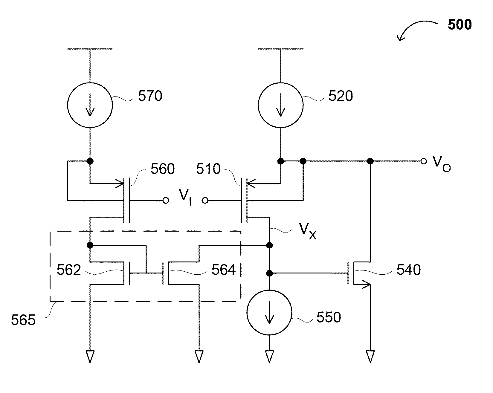
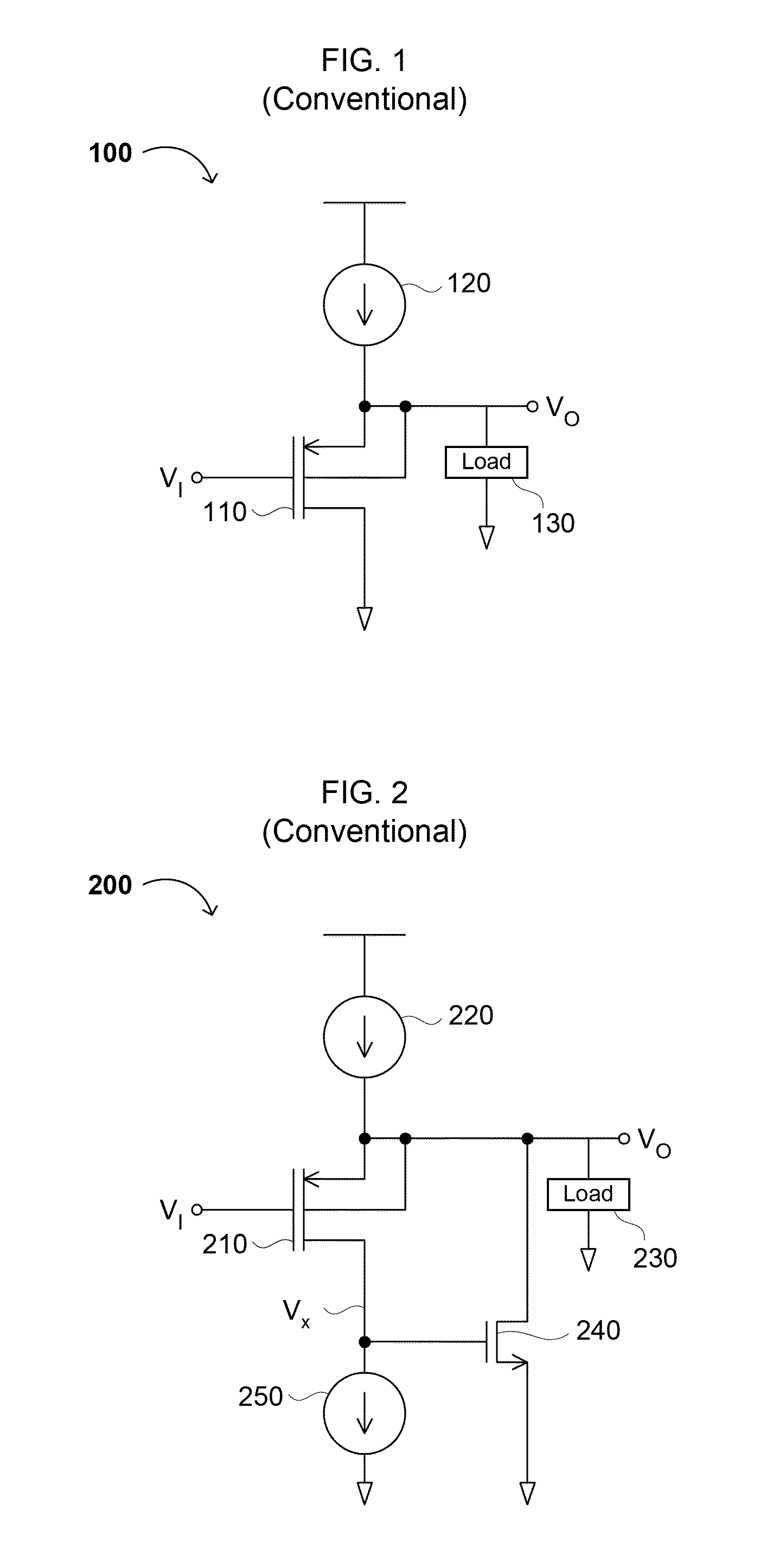
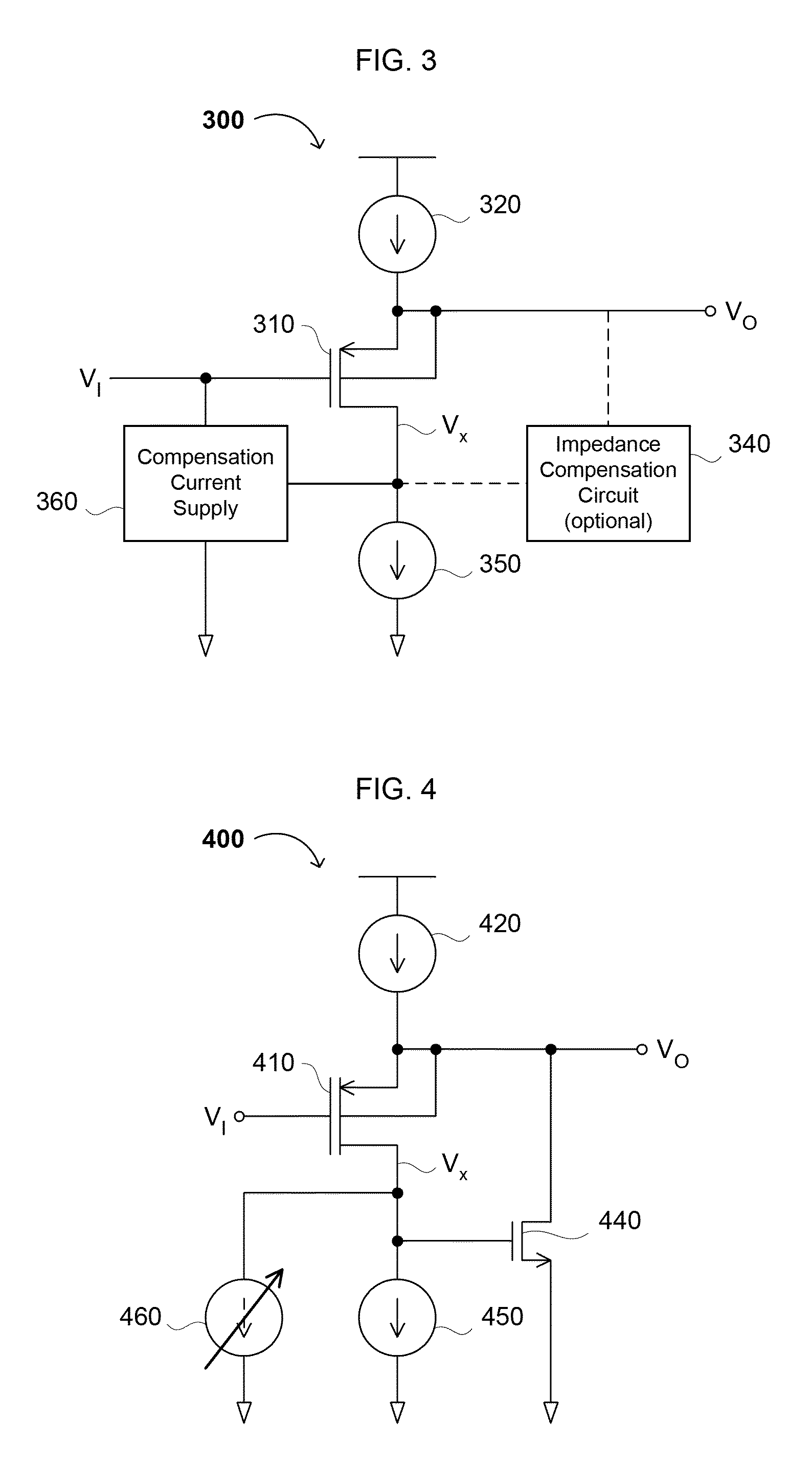
[0028]Reference will now be made in detail to various embodiments of the invention, examples of which are illustrated in the accompanying drawings. While the invention will be described in conjunction with exemplary embodiments provided below, the embodiments are not intended to limit the invention. On the contrary, the invention is intended to cover alternatives, modifications and equivalents that may be included within the scope of the invention as defined by the appended claims. Furthermore, in the following detailed description, numerous specific details are set forth in order to provide a thorough understanding of the present invention. However, the present invention may be practiced without these specific details. In other instances, well-known methods, procedures, components, and circuits have not been described in detail so as not to unnecessarily obscure aspects of the present invention.

[0029]Some portions of the detailed descriptions which follow are presented in terms of ...


PUM


Abstract

Circuits and methods for compensating for an input-dependent gain error in a buffer and/or amplifier circuit, including applying a dynamic current to the input transistor. Circuits generally include a dynamic current supply coupled to a terminal of the input transistor, the dynamic current supply providing a compensating current. The compensating current can have a magnitude equal to the output impedance of the input transistor times a magnitude of the output voltage. The compensating current can be provided via a current mirror, or directly to a terminal of the input transistor. Methods generally include regulating variations in the current through the input transistor by sinking or sourcing a static current and a dynamic current at a terminal of the input transistor. The dynamic current can be regulated in response to a variation in the input signal.

Description

RELATED APPLICATIONS[0001]This application claims the benefit of U.S. Provisional Patent Application No. 61 / 095,813, filed Sep. 10, 2008, incorporated herein by reference in its entirety.FIELD OF THE INVENTION[0002]The present invention generally relates to the field of amplifier and / or buffer circuits. More specifically, embodiments of the present invention pertain to source follower circuits, and to circuits and methods for compensating for input-dependent gain error(s).DISCUSSION OF THE BACKGROUND[0003]Some conventional amplifiers or buffers include transistors in common-drain configurations. These buffers, commonly referred to as source followers, are advantageous over other amplifier or buffer circuits because of their ability to operate at high speed. Such buffers also enable circuits that provide an output having a high current drive from an input having a relatively low current drive capability. Source follower circuits are also commonly used as level-shifting circuits, for ...

Claims


Application Information

Patent Timeline
Patent Type & Authority Patents(United States)
IPC IPC(8): H03G3/30
CPCH03F3/45179H03F3/505H03F2203/5031
Inventor OO, KENNETH THET ZINROO, PIERTE
Owner MARVELL INT LTD
Why Eureka
Try Eureka