Charged particle apparatus, scanning electron microscope, and sample inspection method

a scanning electron microscope and charge particle technology, applied in the direction of material analysis, instruments, and wave/particle radiation material analysis, can solve the problem of not being able to search for the appropriate inspection recipe, and achieve the effect of easy and quick selection

Inactive Publication Date: 2011-09-27
HITACHI HIGH-TECH CORP
View PDF21 Cites 6 Cited by
  • Summary
  • Abstract
  • Description
  • Claims
  • Application Information

AI Technical Summary

Benefits of technology

[0010]This invention, in keeping with the information, has as its goal to be able to quickly and easily select an appropriate recipe for a sample from any of a plurality of inspection recipes.
[0012]According to an embodiment of this invention, plural control parameters is displayed by arrangement on a coordinate system which has, for axes, the characteristic values such as robustness variable of charge up, throughput of defect inspection, and accuracy of defect inspection. Because these characteristic values have relationship trade-offs, the operator can easily and quickly select the inspection recipe that is appropriate for the sample from among plural control parameters that are arranged on the coordinate system.

Problems solved by technology

However, it is not possible to search for an inspection recipe that is appropriate for a sample which is not registered in the database.
However, this technology is directed to determine the charge, and is not directed to select the most appropriate recipe for the sample.

Method used


Image

  • Charged particle apparatus, scanning electron microscope, and sample inspection method
  • Charged particle apparatus, scanning electron microscope, and sample inspection method
  • Charged particle apparatus, scanning electron microscope, and sample inspection method

Examples


Embodiment Construction

[0027]Below, there is an explanation of one embodiment of this invention.

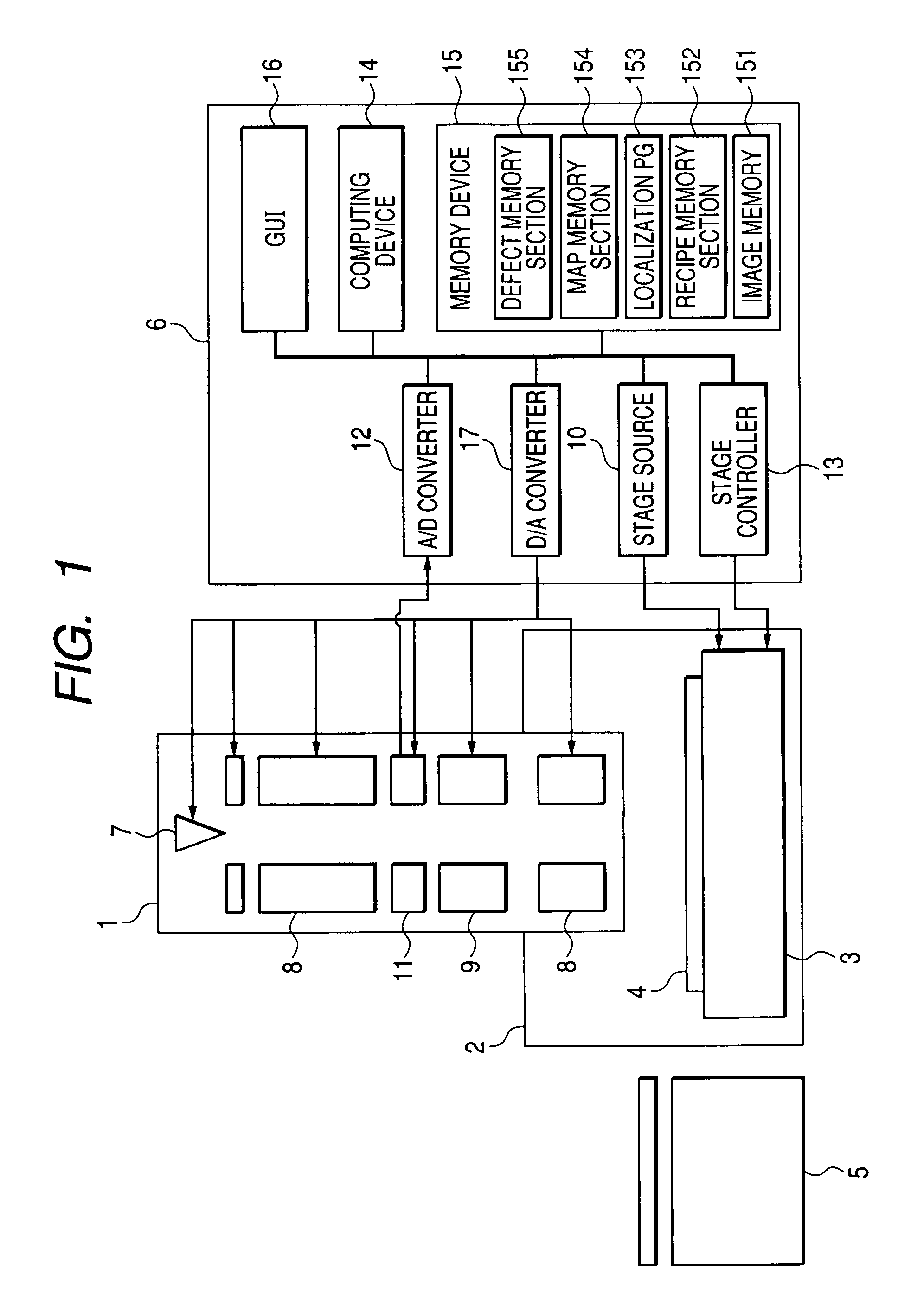
[0028]FIG. 1 is an outline view of the charged particle apparatus which is used for one embodiment of this invention.

[0029]As shown in the FIG., the charged particle beam of this embodiment provides an electronic optical system 1 which irradiates an electron beam on the sample 4, a sample chamber 2, a stage 3 which is placed in the sample chamber 2, a carry structure which carries the sample 4 to the stage 3 of the sample chamber 2, and a control device 6.

[0030]The electron optical system 1 has an electron gun 7 which generates an electron beam, a focusing lens 8 which focuses the electron beam, a deflection lens 9 which deflects the electron beam, and a detector 11 which detects the electrons that are secondarily emitted from the sample 4. The electron gun 7 and the deflection lens 9 form the SEM column, and the focusing lens 8 forms an image optical system.

[0031]The control device 6 has a stage electrical sou...


PUM

PropertyMeasurementUnit
dielectric constantaaaaaaaaaa

Abstract

An object of the invention is to be able to select easily and quickly inspection recipes which are appropriate to samples from any number of inspection recipes. A calculating device displays a plurality of inspection recipes on the GUI. An inspection recipe includes settings for controlling charged particle columns which irradiate charged particles on samples with a plurality of characteristics. Plural inspection recipes are arranged and displayed on a coordinate system which is specified by a plurality of axes having characteristic values (robustness variable of charge up, throughput of defect inspection, and accuracy of defect inspection) which have mutually trade-off relationships.

Description

CLAIM OF PRIORITY[0001]The present application claims priority from Japanese application JP 2006-028720 filed on Feb. 6, 2006, the content of which is hereby incorporated by reference into this application.FIELD OF THE INVENTION[0002]This invention relates to a charged particle apparatus and a scanning electron microscope, and especially to technology which supports the selection of inspection recipes for the charged particle apparatus and scanning electron microscope.BACKGROUND OF THE INVENTION[0003]Conventionally, in order to localize the defects for fine structure formation such as with LSI (Large Scale Integration), various inspection systems are used. For example, optical inspection systems form optical images of minute circuits with the object of inspecting this image in order to detect abnormalities. However, with optical images there is insufficient resolution to specify the minute feature characteristics, and because of that limitation, it is difficult to distinguish damagi...

Claims


Application Information

Patent Timeline
Patent Type & Authority Patents(United States)
IPC IPC(8): G01N23/00G21K7/00A61N5/00
CPCH01J37/263H01J37/265H01J37/28H01J2237/0044H01J2237/0048H01J2237/21H01J2237/2487H01J2237/2817
Inventor FUKUDA, MUNEYUKISHOJO, TOMOYASUFUKADA, ATSUKOTAKAHASHI, NORITSUGU
Owner HITACHI HIGH-TECH CORP
Why Eureka
Try Eureka