Touch sensor, display with touch sensor, and method for generating position data

a technology of touch sensor and display, which is applied in the direction of electric digital data processing, instruments, computing, etc., can solve the problems of expanding the range of non-effective locations where no location sensing can be carried out, and achieves the effects of reducing thickness, saving power dissipation, and small parallax

Active Publication Date: 2011-10-04
SHARP KK +1
View PDF27 Cites 157 Cited by
  • Summary
  • Abstract
  • Description
  • Claims
  • Application Information

AI Technical Summary

Benefits of technology

[0015]In order to overcome the problems described above, an object of the present invention is to provide a touch sensor, which does not deteriorate display performance and which is lightweight and contributes to downsizing effectively, a display device with such a touch sensor, and a method of generating location data.
[0054]This display device with a touch sensor is provided with no additional transparent conductive film for locating a point of contact of a pen or a finger with a display plane by an electrostatic capacitive coupling technique. Instead, in this display device, one of the first and second circuits is electrically connected to the transparent counter electrode by a switching circuit, thereby using the transparent counter electrode for a display panel on a time-sharing basis and locating the point of contact. Thus, the deterioration in display quality, which should be caused when such an additional transparent conductive film is provided on the front side of a display device, is avoidable. Also, this display device with a touch sensor can have reduced size and weight.
[0055]If the switching circuit, as well as a display driver circuit and a location sensor circuit, is made up of thin-film transistors that are provided on the substrate, then high-speed switching is achieved. As a result, the delay in the application of a display voltage, which might be caused during switching, can be minimized.
[0057]In this touch sensor, the Y coordinate detecting conductive portion and the X coordinate detecting conductive portion are electrically connected to the first and second location sensing transparent conductive films, respectively. Accordingly, compared with a conventional touch sensor, including just one transparent conductive film provided with a conductive portion for sensing locations in the Y-axis and X-axis directions, the coordinate detecting conductive portions can have simplified patterns. That is to say, each of the coordinate detecting conductive portions occupies a smaller area on its associated transparent conductive film, and therefore, the operating plane can have an increased contact point locatable area.
[0058]Also, the switching circuit alternately makes one of the first and second location sensing transparent conductive films electrically conductive, thereby detecting the Y and X coordinates independent of each other. Accordingly, the detection of one of these two coordinates is not affected by that of the other coordinate. As a result, the coordinates of any location can be detected accurately.
[0061]Accordingly, there is no need to provide a wide gap between the location sensing transparent conductive film and the electrode. Also, no shielding layer needs to be provided between the display panel and the location sensing transparent conductive film, either. As a result, a display device with a touch sensor that can have a reduced thickness and that causes small parallax can be provided. Furthermore, in locating the point of contact, no special voltage is applied to the location sensing transparent conductive film but the induced voltage, generated by applying the periodically changing oscillating voltage to the electrode, is used. Thus, no complicated circuit is needed and the power dissipation never increases, either. Furthermore, a voltage, which is essentially supplied to a display panel to drive its display medium layer, may be used as such an oscillating voltage. In addition, no alternating current voltage needs to be separately applied to the location sensing transparent conductive film, thus saving the power dissipation.

Problems solved by technology

If the conductive pattern gets complicated, however, then the non-effective range where no location sensing can be carried out expands.

Method used


Image

  • Touch sensor, display with touch sensor, and method for generating position data
  • Touch sensor, display with touch sensor, and method for generating position data
  • Touch sensor, display with touch sensor, and method for generating position data

Examples


embodiment 1

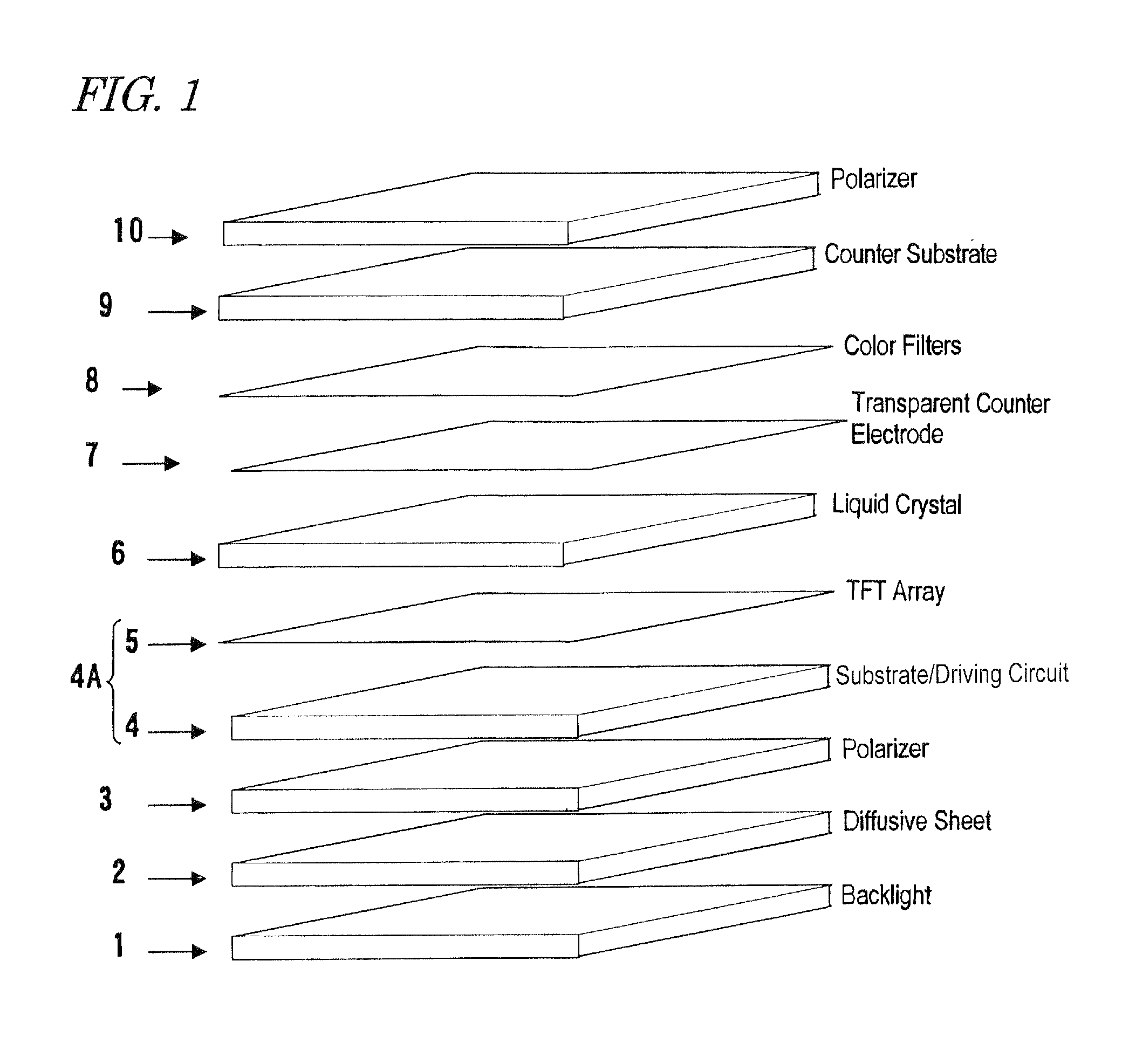
[0086]First, a display device with a touch sensor according to an embodiment of the present invention will be described with reference to FIG. 1. FIG. 1 schematically shows a configuration in which a display device with a touch sensor according to the present invention is applied to a liquid crystal display device. As shown in FIG. 1, a backlight 1, a diffusive sheet 2, a first polarizer 3, a substrate (i.e., first substrate) 4, a TFT array 5, a liquid crystal layer 6, a transparent counter electrode 7, color filters 8, a counter substrate (i.e., second substrate) 9 and a second polarizer 10 are stacked in this order one upon the other.

[0087]Hereinafter, a configuration for a liquid crystal display device with a touch sensor according to this first embodiment will be described in further detail.

[0088]The TFT array 5 is provided, and pixel electrodes (not shown) are arranged in matrix, on the first surface of the substrate 4, which is made of a transparent insulating material such as...

embodiment 2

[0138]Hereinafter, a touch sensor according to another embodiment of the present invention will be described with reference to FIGS. 12 and 13.

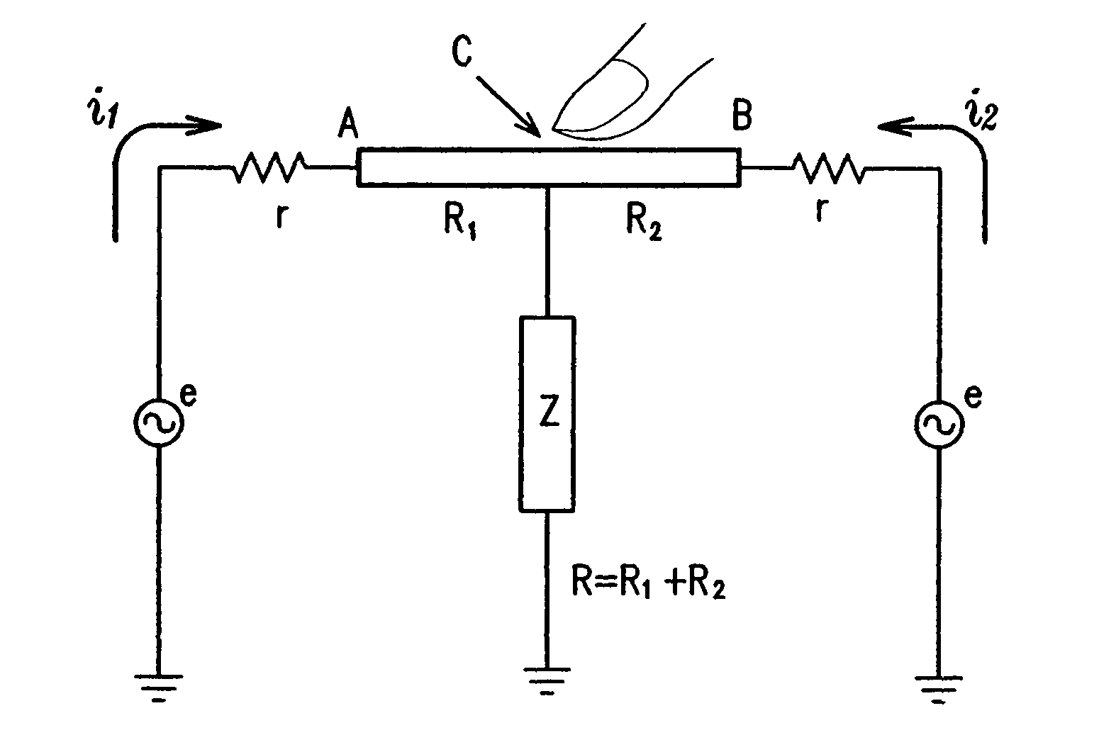
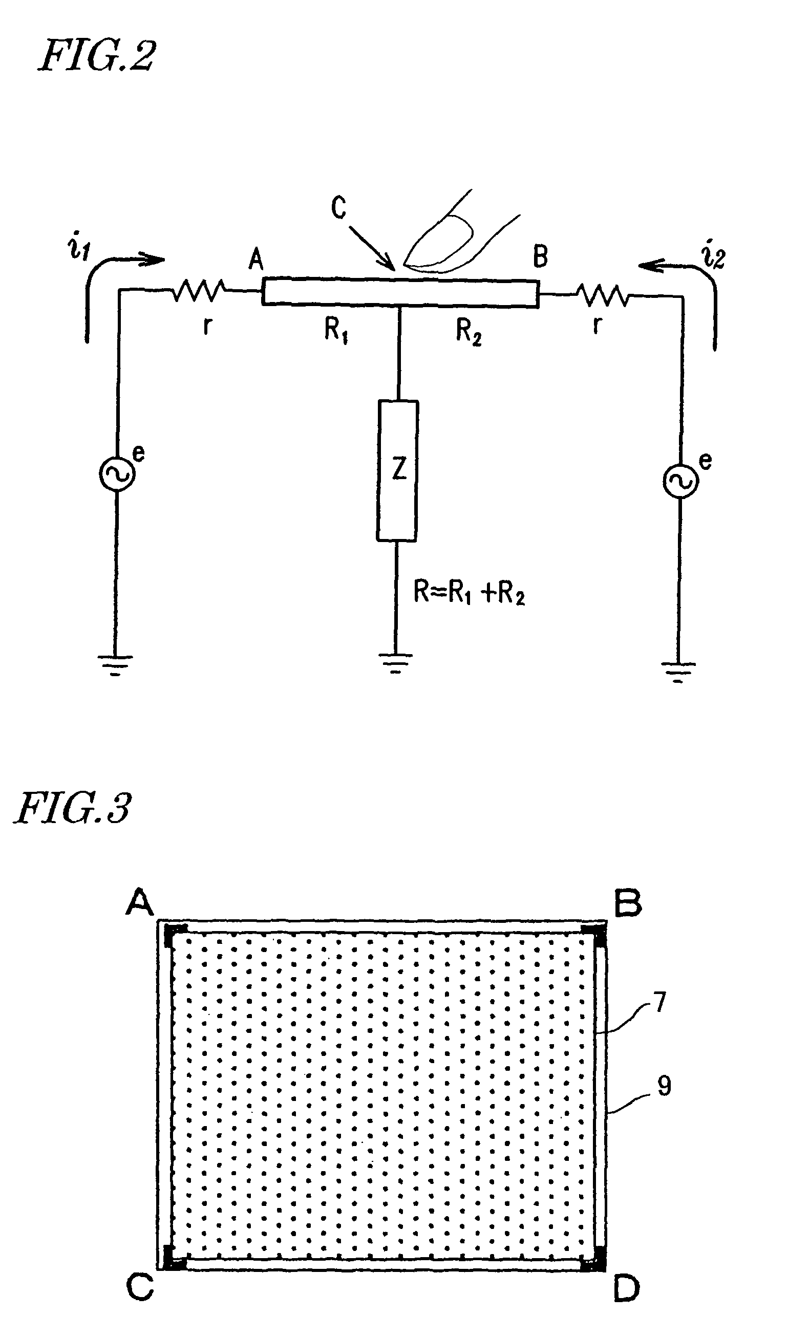
[0139]A touch sensor 37 according to this second preferred embodiment detects an external input point on a two-dimensional operating plane (i.e., extending in X and Y directions) by an electrostatic capacitive coupling technique. In the following preferred embodiment, a situation where an input point is defined by touching the operating plane with a finger or an electrically conductive pen, for example, will be described. FIG. 12 is a perspective view schematically illustrating a configuration for the touch sensor 37.

[0140]As shown in FIG. 12, the touch sensor 37 includes: two location sensing transparent conductive films (or transparent resistive films), i.e., a first location sensing transparent conductive film 32 arranged parallel to the operating plane and a second location sensing transparent conductive film 34 arranged so as to face the...

embodiment 3

[0184]Hereinafter, a display device with a touch sensor according to another preferred embodiment of the present invention will be described with reference to FIG. 17.

[0185]FIG. 17 schematically illustrates a configuration for a display device 53 with a touch sensor according to a third preferred embodiment of the present invention.

[0186]The display device 53 with a touch sensor includes a display panel 49, a location sensing transparent conductive film 47, and a sensor circuit (not shown in FIG. 17).

[0187]The display panel 49 includes at least a display medium layer 44, a transparent counter electrode 45, which is provided closer to the viewer than the display medium layer 44 is so as to drive the display medium layer 44, and an insulating layer (dielectric layer) 46, which is provided closer to the viewer than the transparent counter electrode 45 is. The location sensing transparent conductive film 47 is arranged so as to face the transparent counter electrode 45 with the insulati...


PUM

PropertyMeasurementUnit
voltageaaaaaaaaaa
voltageaaaaaaaaaa
voltageaaaaaaaaaa

Abstract

A display device with a touch sensor according to the present invention includes an active matrix substrate 4A and a transparent counter electrode 7. On a first surface of the active matrix substrate, multiple pixel electrodes are arranged in matrix. The transparent counter electrode is opposed to the first surface of the active matrix substrate. The display device further includes a first circuit, a second circuit and a switching circuit. The first circuit supplies a voltage or a current to the transparent counter electrode for display purposes. The second circuit detects currents flowing from a number of points on the transparent counter electrode. And the switching circuit selectively connects electrically one of the first and second circuits to the transparent counter electrode.

Description

[0001]This application is the US national phase of international application PCT / JP02 / 07331 filed 18 Jul. 2002, which designated the US. PCT / JP2 / 07331 claims priority to JP Application No. 2001-252076 filed 22 Aug. 2001, JP Application No. 2001-371246 filed 05 Dec. 2001 and JP Application No. 2002-171739 filed 12 Jun. 2002. The entire contents of these applications are incorporated herein by reference.TECHNICAL FIELD[0002]The present invention relates to a touch sensor which can locate a point on a display plane that has been touched with a pen or a finger, a display device with such a touch sensor, and a method of generating location data.BACKGROUND ART[0003]A touch sensor is an input device for sensing a point that has been touched with a finger or a pen. Examples of known location sensing techniques include electrostatic capacitive coupling type, a resistive film type, an infrared ray type, an ultrasonic type, and electromagnetic induction / coupling type. Among other things, touch...

Claims


Application Information

Patent Timeline
Patent Type & Authority Patents(United States)
IPC IPC(8): G06F3/041G02F1/133G06F3/044G06F3/045
CPCG06F3/0412G06F3/044G06F3/045G02F1/13338G06F2203/04113G06F3/0443G06F3/0444G06F3/0446
Inventor MIYAMOTO, SABURONAKANO, TOSHIHISA
Owner SHARP KK
Why Eureka
Try Eureka