Touch sensor, display with touch sensor, and method for generating position data

Active Publication Date: 2004-11-04
SHARP KK +1
View PDF14 Cites 314 Cited by
  • Summary
  • Abstract
  • Description
  • Claims
  • Application Information

AI Technical Summary

Benefits of technology

0014] In order to overcome the problems described above, an object of the present invention is to provide a touch sensor, which does not deteriorate display per

Problems solved by technology

If the conductive pattern gets complicated, however, then the non-e

Method used


Image

  • Touch sensor, display with touch sensor, and method for generating position data
  • Touch sensor, display with touch sensor, and method for generating position data
  • Touch sensor, display with touch sensor, and method for generating position data

Examples


first embodiment

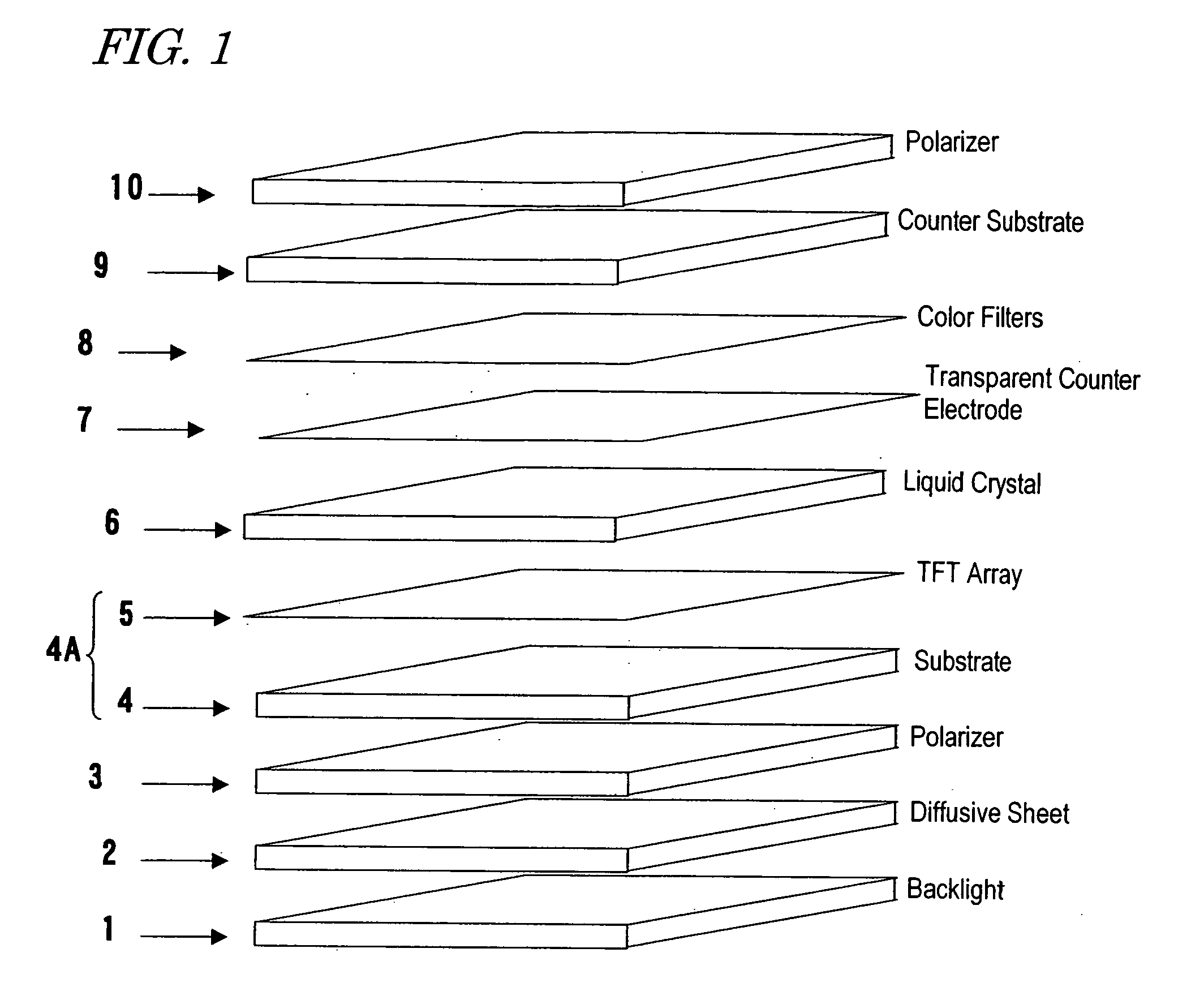
[0086] Hereinafter, a configuration for a liquid crystal display device with a touch sensor according to this first embodiment will be described in further detail.

[0087] The TFT array 5 is provided, and pixel electrodes (not shown) are arranged in matrix, on the first surface of the substrate 4, which is made of a transparent insulating material such as glass or plastic. The pixel electrodes are driven by an active-matrix addressing technique. For that reason, the substrate 4A, obtained by providing the TFT array 5 and others on the surface of the substrate 4, will be referred to herein as an "active-matrix substrate".

[0088] The TFT array 5 on the substrate 4 is an array of thin-film transistors (TFTs), each including a semiconductor thin layer of amorphous silicon or polysilicon, for example. The substrate 4 actually has a peripheral area surrounding the display area. In the peripheral area, driver circuits (i.e., a gate driver and a source driver) are provided to drive pixel TFTs ...

embodiment 2

[0142] Hereinafter, a touch sensor according to another embodiment of the present invention will be described with reference to FIGS. 12 and 13.

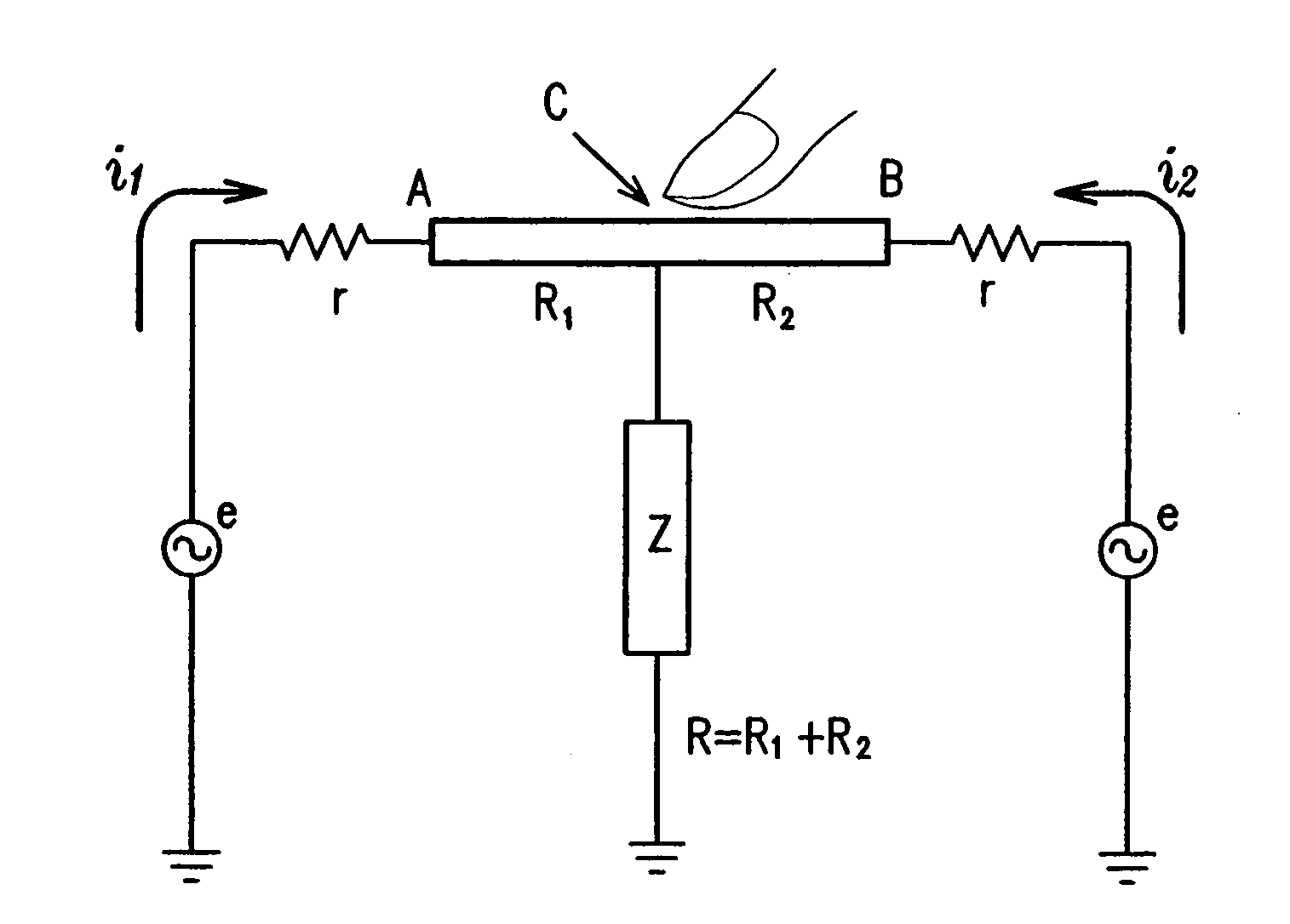
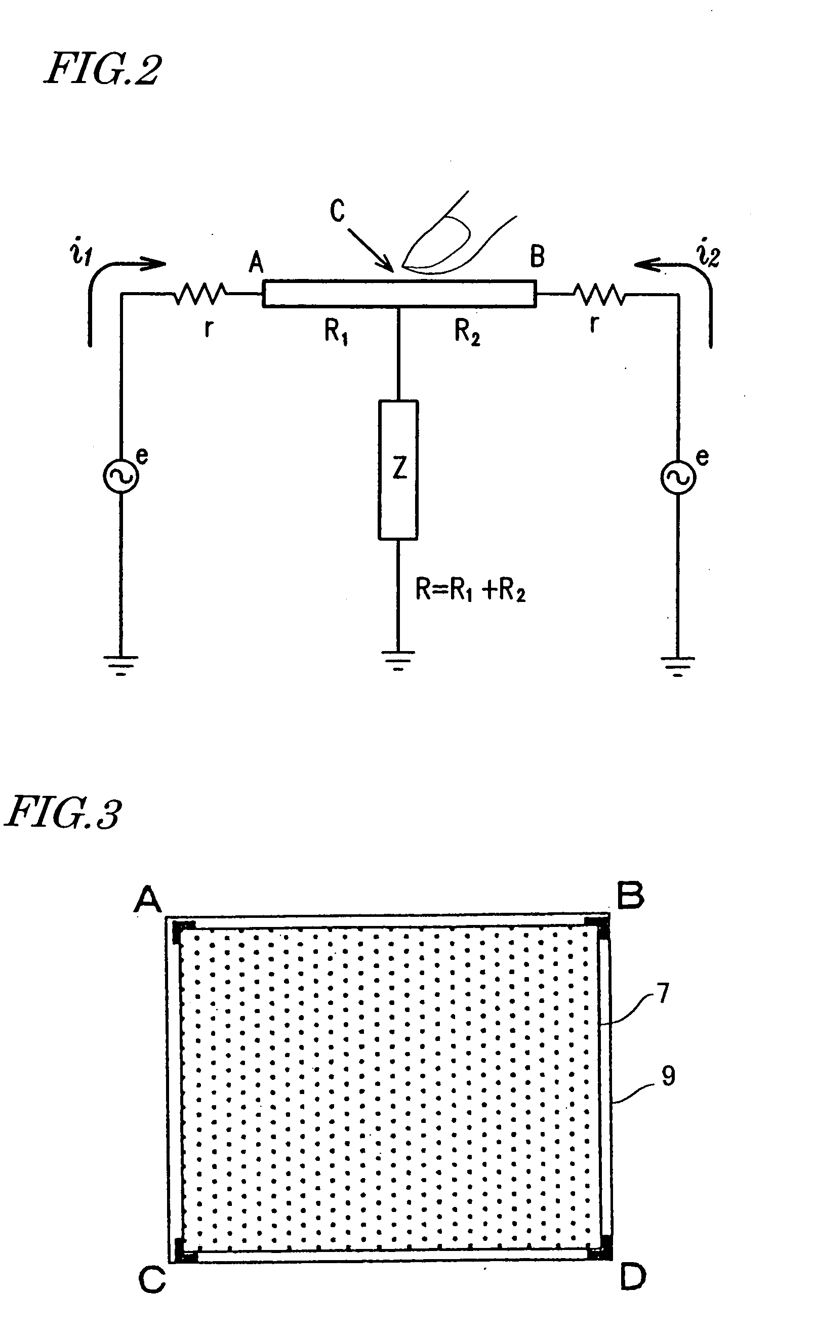
[0143] A touch sensor 37 according to this second preferred embodiment detects an external input point on a two-dimensional operating plane (i.e., extending in X and Y directions) by an electrostatic capacitive coupling technique. In the following preferred embodiment, a situation where an input point is defined by touching the operating plane with a finger or an electrically conductive pen, for example, will be described. FIG. 12 is a perspective view schematically illustrating a configuration for the touch sensor 37.

[0144] As shown in FIG. 12, the touch sensor 37 includes: two location sensing transparent conductive films (or transparent resistive films), i.e., a first location sensing transparent conductive film 32 arranged parallel to the operating plane and a second location sensing transparent conductive film 34 arranged so as to face ...

embodiment 3

[0188] Hereinafter, a display device with a touch sensor according to another preferred embodiment of the present invention will be described with reference to FIG. 17.

[0189] FIG. 17 schematically illustrates a configuration for a display device 53 with a touch sensor according to a third preferred embodiment of the present invention.

[0190] The display device 53 with a touch sensor includes a display panel 49, a location sensing transparent conductive film 47, and a sensor circuit (not shown in FIG. 17).

[0191] The display panel 49 includes at least a display medium layer 44, a transparent counter electrode 45, which is provided closer to the viewer than the display medium layer 44 is so as to drive the display medium layer 44, and an insulating layer (dielectric layer) 46, which is provided closer to the viewer than the transparent counter electrode 45 is. The location sensing transparent conductive film 47 is arranged so as to face the transparent counter electrode 45 with the insu...


PUM


Abstract

A display device with a touch sensor according to the present invention includes an active matrix substrate 4A and a transparent counter electrode 7. On a first surface of the active matrix substrate, multiple pixel electrodes are arranged in matrix. The transparent counter electrode is opposed to the first surface of the active matrix substrate. The display device further includes a first circuit, a second circuit and a switching circuit. The first circuit supplies a voltage or a current to the transparent counter electrode for display purposes. The second circuit detects currents flowing from a number of points on the transparent counter electrode. And the switching circuit selectively connects electrically one of the first and second circuits to the transparent counter electrode.

Description

[0001] The present invention relates to a touch sensor which can locate a point on a display plane that has been touched with a pen or a finger, a display device with such a touch sensor, and a method of generating location data.[0002] A touch sensor is an input device for sensing a point that has been touched with a finger or a pen. Examples of known location sensing techniques include electrostatic capacitive coupling type, a resistive film type, an infrared ray type, an ultrasonic type, and electromagnetic induction / coupling type. Among other things, touch sensors of the resistive film type or electrostatic capacitive coupling type are used extensively.[0003] Hereinafter, a touch sensor of the resistive film type will be described. As shown in FIG. 22, a touch sensor of an analog resistive film type includes two transparent resistive films 12 and 14 facing each other with an air layer 13 interposed between them, a PET film 11 provided on the opposite side of the transparent resis...

Claims


Application Information

Patent Timeline
IPC IPC(8): G02F1/133G06F3/041G06F3/044G06F3/045
CPCG02F1/13338G06F3/0412G06F3/044G06F3/045G06F2203/04113G06F3/0443G06F3/0444G06F3/0446
Inventor MIYAMOTO, SABURONAKANO, TOSHIHISA
Owner SHARP KK
Why Eureka
Try Eureka