Circuit for reading a charge retention element for a time measurement

a charge retention element and time measurement technology, applied in the field of electronic circuits, can solve the problems of limited measurable time range and inability to easily compatible with memory manufacturing steps, and the solution of the above-mentioned document is known

Active Publication Date: 2011-10-11
STMICROELECTRONICS SRL
View PDF16 Cites 31 Cited by
  • Summary
  • Abstract
  • Description
  • Claims
  • Application Information

AI Technical Summary

Benefits of technology

[0014]At least one embodiment of the present invention aims at overcoming all or part of the disadvantages of known solutions to provide data representative of a time elapsed between two events, without it being necessary to permanently power the electronic circuit containing the means to achieve this.
[0018]According to a fourth aspect, at least one embodiment of the present invention aims at a fast programming of an electronic charge retention circuit.

Problems solved by technology

First, the measurable time range is limited by the possibilities of intervention on the capacitive component dielectric.
The known solution of the above-mentioned document is not easily compatible with the memory manufacturing steps.

Method used


Image

  • Circuit for reading a charge retention element for a time measurement
  • Circuit for reading a charge retention element for a time measurement
  • Circuit for reading a charge retention element for a time measurement

Examples


first embodiment

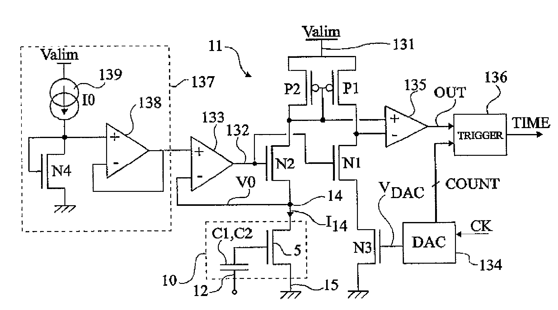
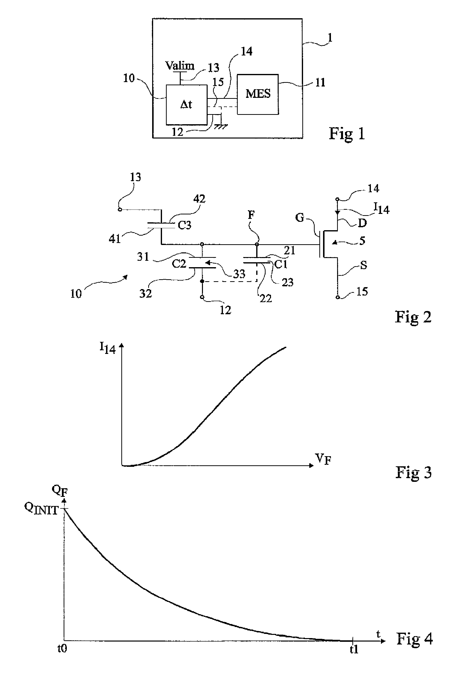
[0052]FIG. 2 shows the electric diagram of a controllable charge retention circuit 10 according to the first aspect of the present invention.

[0053]Circuit 10 comprises a first capacitive element C1 having a first electrode 21 connected to a floating node F and having its dielectric spacer 23 designed (by its permittivity and / or by its thickness) to have leakages which are not negligible with time. “Floating node F” is used to designate a node which is not directly connected to any diffused region of the semiconductor substrate and, more specifically, which is separated by a dielectric spacer, from any voltage-application terminal. By default, second electrode 22 of capacitive element C1 is either connected (dotted lines in FIG. 2) to terminal 12 intended to be connected to a reference voltage, or left unconnected.

[0054]A second capacitive element C2 has a first electrode 31 connected to node F and a second electrode 32 connected to terminal 12. Dielectric spacer 33 of capacitive ele...

second embodiment

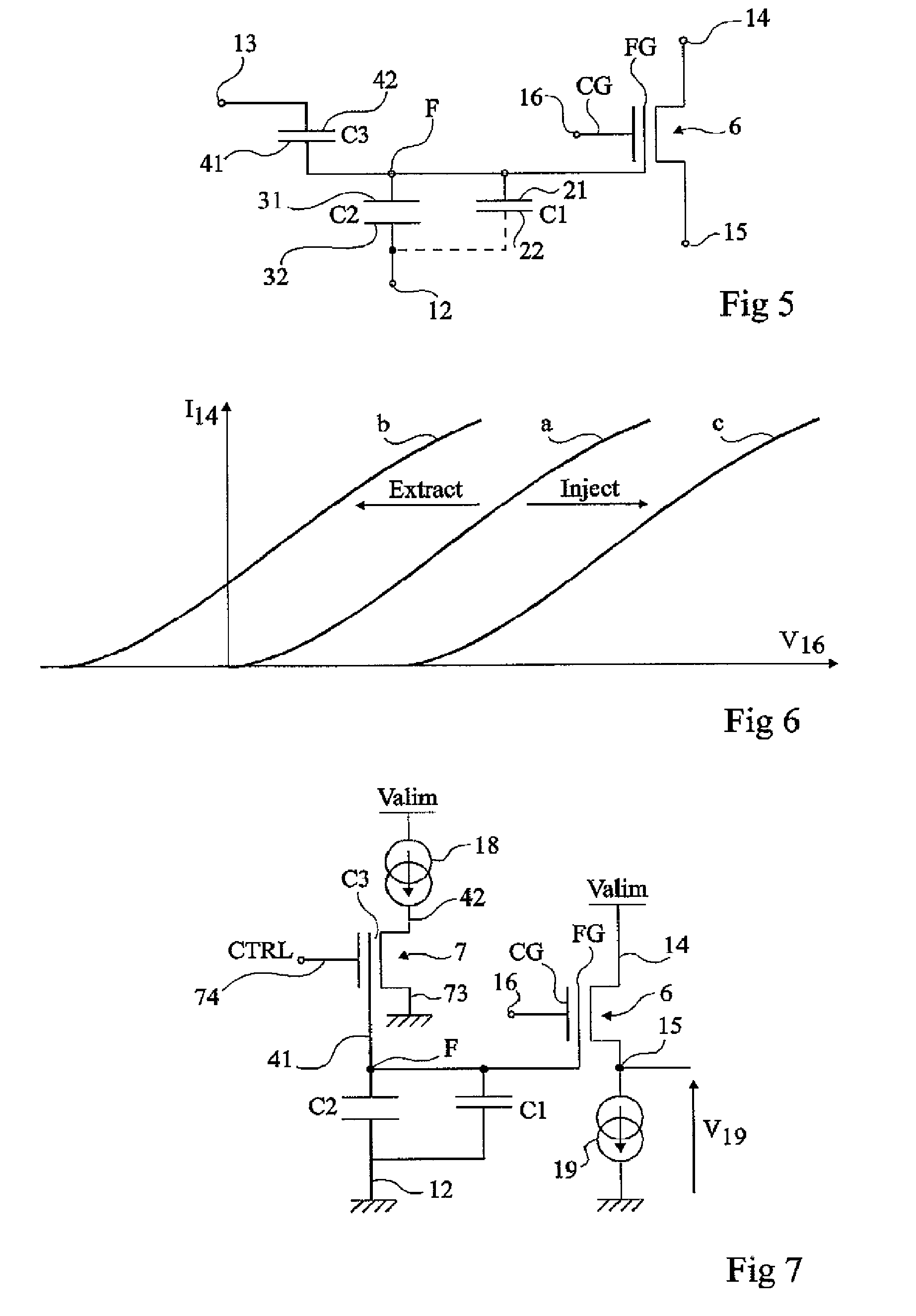
[0067]FIG. 5 shows a circuit according to the present invention. As compared with the embodiment of FIG. 2, transistor 5 is replaced with a transistor 6 with a floating gate FG connected to node F. Control gate CG of transistor 6 is connected to a terminal 16 of control in read mode of the residual charge in the circuit.

[0068]FIG. 6 illustrates, in a graph of current I14 versus voltage V16 applied on the control gate, the operation of the circuit of FIG. 5. It is assumed that the voltage at drain and source terminals 14 and 15 of transistor 6 is maintained constant by an external read circuit (11, FIG. 1). The voltage drop between the floating gate and terminal 15 then depends on the electric charge present at node F, on the total capacitance between nodes F and 12 (essentially capacitances C1 and C2), and on the voltage applied on control terminal 16 of transistor 6. In FIG. 6, three curves a, b, and c have been illustrated. Curve a shows the case where node F is totally discharged...


PUM


Abstract

A method and a circuit for reading an electronic charge retention element for a temporal measurement, of the type including at least one capacitive element whose dielectric exhibits a leakage and a transistor with insulated control terminal for reading the residual charges, the reading circuit including; two parallel branches between two supply terminals, each branch including at least one transistor of a first type and one transistor of a second type, the transistor of the second type of one of the branches consisting of that of the element to be read and the transistor of the second type of the other branch receiving, on its control terminal, a staircase signal, the respective drains of the transistors of the first type being connected to the respective inputs of a comparator whose output provides an indication of the residual voltage in the charge retention element.

Description

BACKGROUND OF THE INVENTION[0001]1. Field of the Invention[0002]The present invention generally relates to electronic circuits and, more specifically, to the forming of a circuit enabling controllably storing electric charges for a time measurement.[0003]2. Discussion of the Related Art[0004]In many applications, it is desired to have data representative of a time elapsed between two events, be it an accurate or approximate measurement. An example of application relates to the time management of rights of access, especially to media.[0005]The obtaining of such data representative of the elapsed time conventionally requires a time measurement by an electronic circuit powered, for example by means of a battery, to avoid losing the history of the data when the circuit is not used.[0006]It would be desirable for a time measurement which operates even when the electronic measurement circuit is not powered to be available.[0007]International patent WO-A-03 / 083769 describes a time-measurem...

Claims


Application Information

Patent Timeline
Patent Type & Authority Patents(United States)
IPC IPC(8): G11C11/24
CPCG11C7/06G11C7/062G04F10/10
Inventor LA ROSA, FRANCESCO
Owner STMICROELECTRONICS SRL
Why Eureka
Try Eureka