Method and apparatus for separating protective tape from semiconductor wafer

a technology of protective tape and semiconductor wafer, which is applied in the direction of semiconductor/solid-state device testing/measurement, mechanical control devices, instruments, etc., can solve the problems of increasing damage, reducing strength, and frequent damage to the wafer, and achieve the effect of preventing further growth of defects

Inactive Publication Date: 2011-10-18
NITTO DENKO CORP
View PDF8 Cites 0 Cited by
  • Summary
  • Abstract
  • Description
  • Claims
  • Application Information

AI Technical Summary

Benefits of technology

[0008]The present invention is directed to appropriately separate a protective tape from a semiconductor wafer while preventing further growth of a defect such as a chip or a crack on an outer periphery of the semiconductor wafer.

Problems solved by technology

In the case where the protective tape is separated from the thinned wafer, the wafer is frequently damaged from a stress to be applied thereto when the protective tape is joined thereto or separated therefrom, because of reduction in strength.
In the back grinding process, particularly, such a stress causes further growth of a defect such as a chip or a crack on an outer periphery of the wafer, resulting in increase of the damage.
If the wafer is further damaged by the growth of the defect and, consequently, the protective tape can not be separated from the wafer because of the damage, the wafer is discarded before being subjected to the dicing process.
For this reason, all the chip components including usable non-defectives are discarded, so that there arises a problem of reduction in yield.

Method used


Image

  • Method and apparatus for separating protective tape from semiconductor wafer
  • Method and apparatus for separating protective tape from semiconductor wafer
  • Method and apparatus for separating protective tape from semiconductor wafer

Examples


Embodiment Construction

[0030]The present invention is described more fully hereinafter with reference to the accompanying drawings, in which embodiments of the invention are shown. The invention may, however, be embodied in many different forms and should not be construed as limited to the embodiments set forth herein. Rather, these embodiments are provided so that this disclosure is thorough, and will fully convey the scope of the invention to those skilled in the art. In the drawings, the size and relative sizes of layers and regions may be exaggerated for clarity. Like reference numerals in the drawings denote like elements.

[0031]One exemplary embodiment of the present invention will be described in detail hereinafter with reference to the drawings.

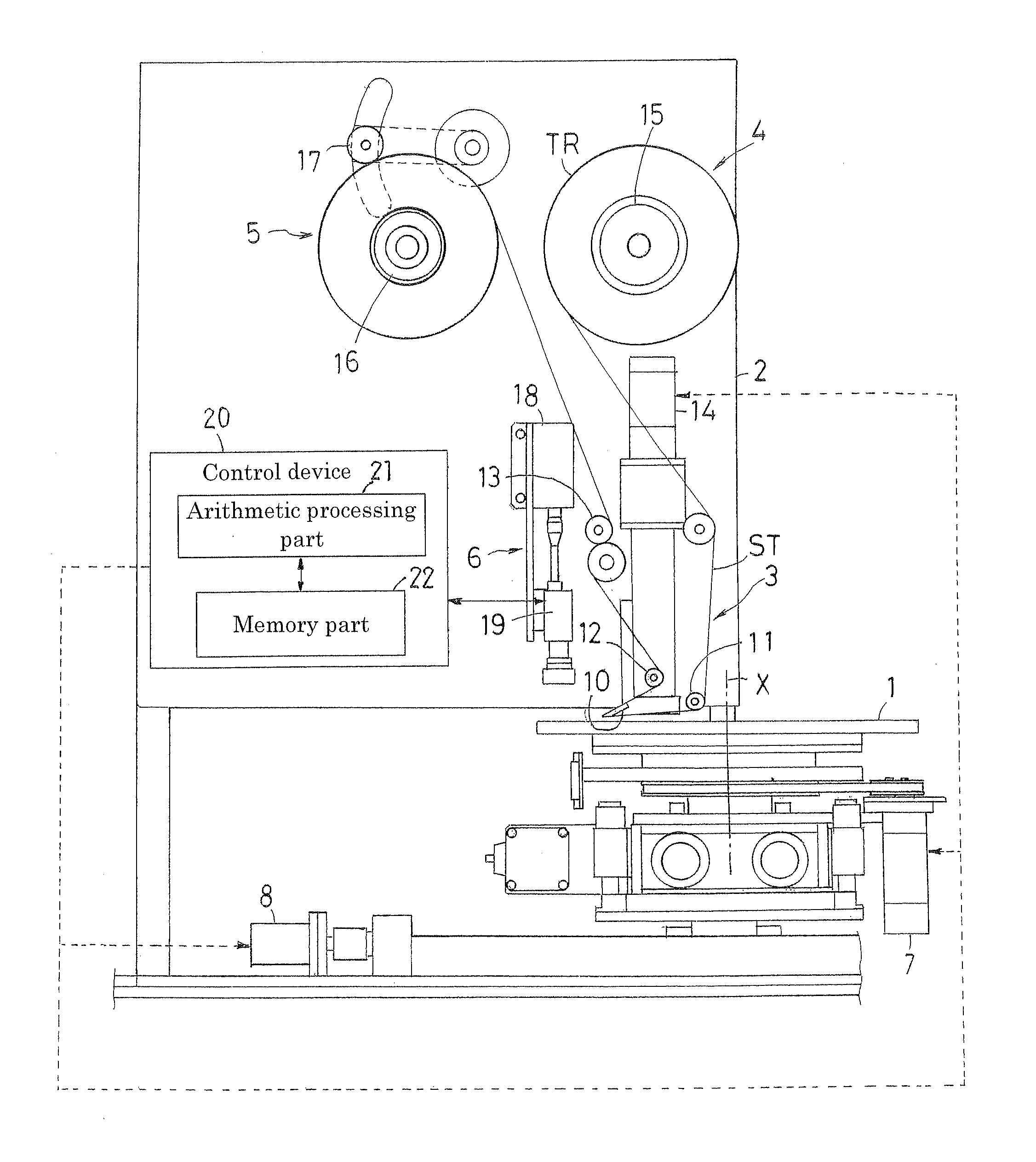
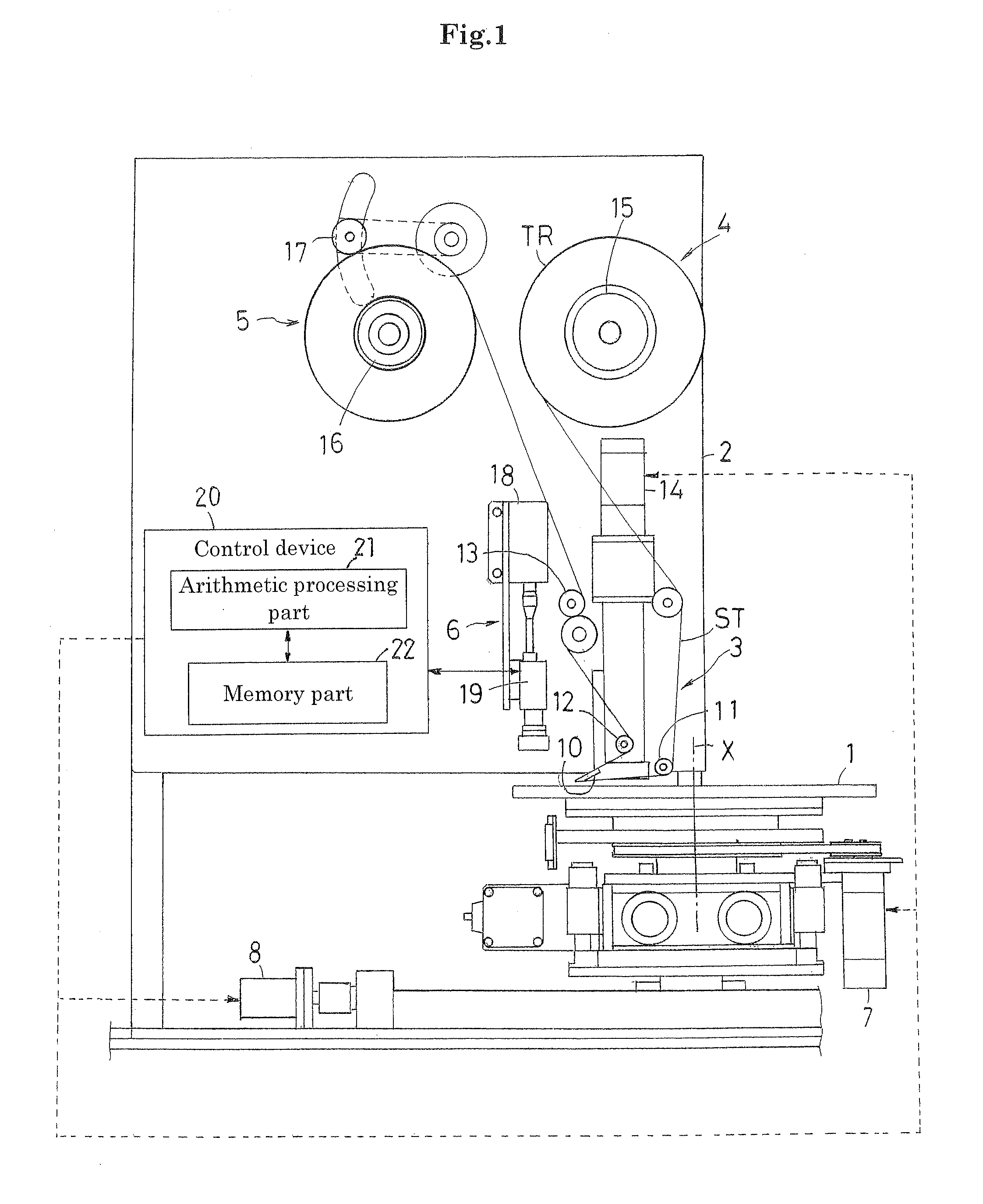
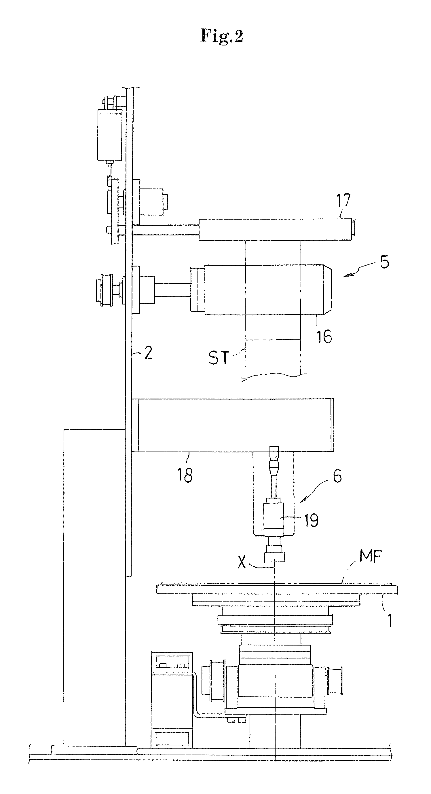
[0032]FIG. 1 shows a front view of a protective tape separating apparatus that implements a method according to the present invention. FIG. 2 shows a side view of the protective tape separating apparatus.

[0033]The protective tape separating apparatus include...


PUM

PropertyMeasurementUnit
diameteraaaaaaaaaa
widthaaaaaaaaaa
areaaaaaaaaaaa

Abstract

A method of this invention involves capturing an image of an outer periphery of a semiconductor wafer, by use of a CCD camera, performing image analysis on data about the captured image, detecting defects such as chips and cracks on the outer periphery of the semiconductor wafer, storing positions of the respective defects, calculating a clearance between the adjacent defects from information about the stored positions, comparing the calculated clearances with a preset width of a separation tape, and obtaining the clearance larger than the width of the separation tape, by arithmetic processing. If some of the clearances are larger than the width of the separation tape, this method also involves setting an appropriate one of the clearance as a position where the separation tape is joined, performing alignment on the semiconductor wafer, joining the separation tape to a protective tape joined to a surface of the semiconductor wafer, and separating the protective tape together with the separation tape from the surface of the semiconductor wafer.

Description

BACKGROUND OF THE INVENTION[0001]1. Field of the Invention[0002]The present invention relates to a method and an apparatus for joining, to a protective tape joined to a surface of a semiconductor wafer, a separation tape having a width narrower than a diameter of the semiconductor wafer to separate the protective tape together with the separation tape from the surface of the semiconductor wafer.[0003]2. Description of the Related Art[0004]Conventionally, a chip component has been manufactured from a semiconductor wafer (hereinafter, appropriately referred to as a “wafer”) in accordance with the following procedure.[0005]As disclosed in JP2002-124494A, for example, a circuit pattern is formed on a surface of a wafer, and then a protective tape is joined to the surface of the wafer. Thereafter, a back grinding process is performed on a rear face of the wafer in order to thin the wafer. The thinned wafer is held by a ring frame through a dicing tape. In this state, the protective tape ...

Claims


Application Information

Patent Timeline
Patent Type & Authority Patents(United States)
IPC IPC(8): B32B38/00B32B41/00
CPCB32B37/0046B32B38/10B32B41/00H01L21/67132H01L22/12H01L22/20H01L21/67288B32B2457/14Y10T156/1052Y10T156/108Y10T156/1062H01L21/48
Inventor YAMAMOTO, MASAYUKIHASE, YUKITOSHI
Owner NITTO DENKO CORP
Why Eureka
Try Eureka