Silicon-containing resist underlayer coating forming composition for forming photo-crosslinking cured resist underlayer coating
a technology of resist and composition, applied in the field of composition for forming an underlayer coating, can solve the problems of difficult application of organic materials for difficult to achieve the effect of anti-reflective coating on a substrate having a high aspect ratio, and pollution of the peripheral apparatus due to volatilization or sublimation of components
- Summary
- Abstract
- Description
- Claims
- Application Information
AI Technical Summary
Benefits of technology
Problems solved by technology
Method used
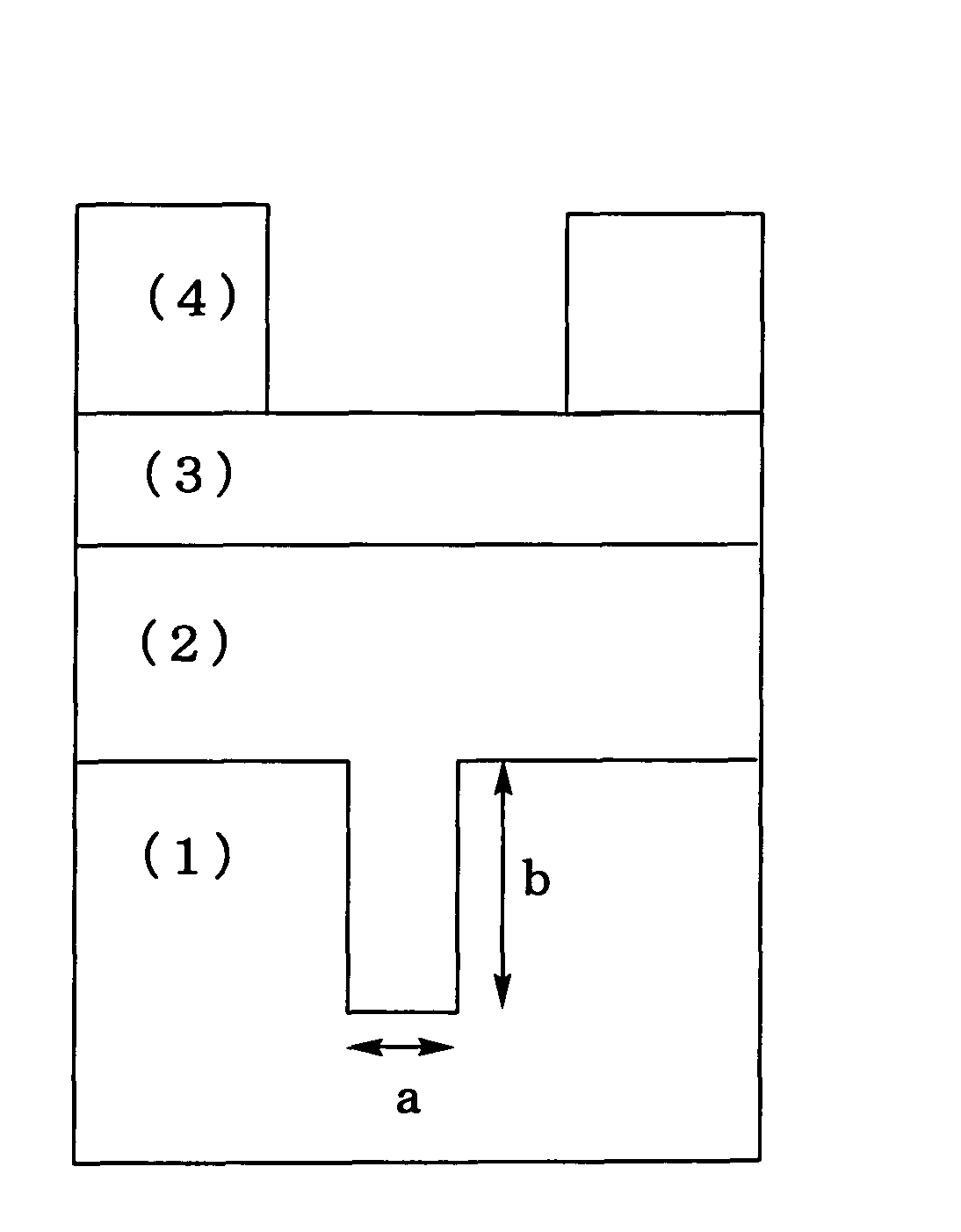
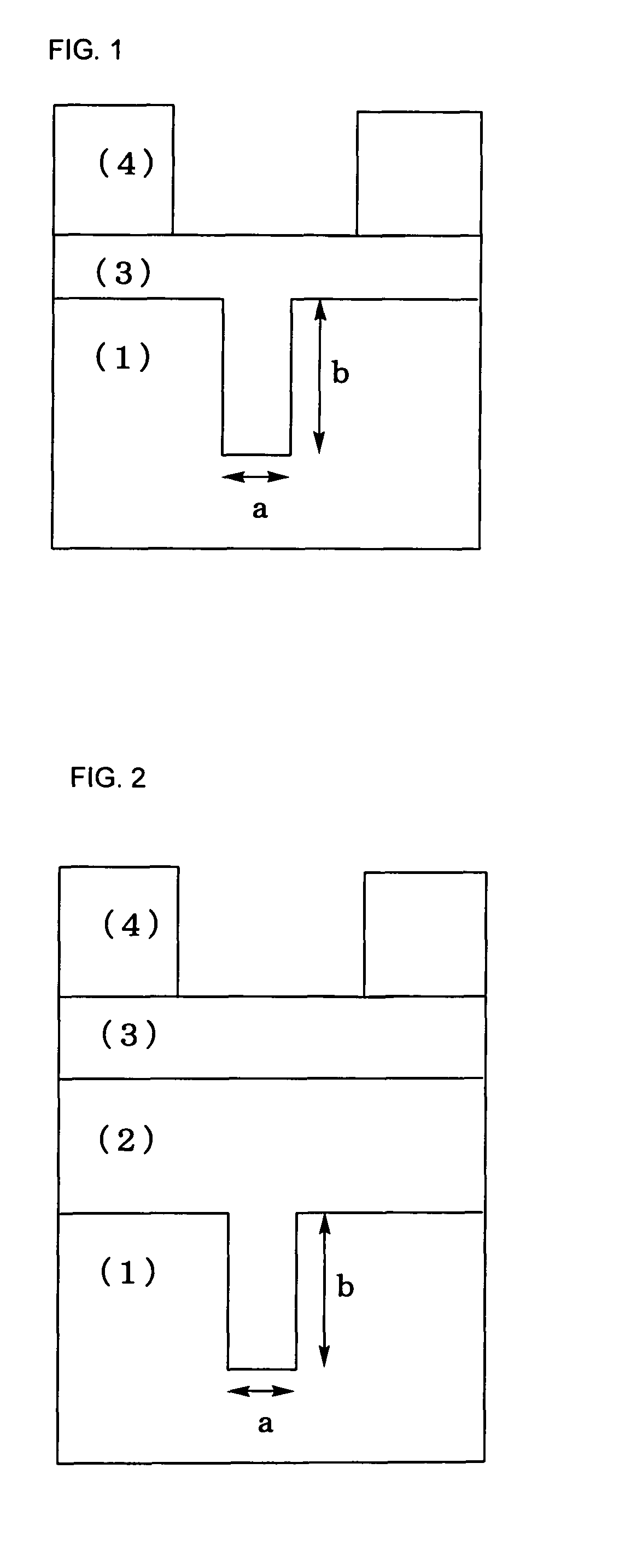
Image

Examples
example 1
[0124]To 19.32 g of ethyl lactate, 2.0 g of 3-(acryloxypropyl) trimethoxy silane (manufactured by AZmax.co.), 0.0768 g of water and 0.147 g of p-toluenesulfonic acid were added and stirred for 3 hours at room temperature to hydrolyze 3-(acryloxypropyl) trimethoxy silane and to obtain a condensate thereof.
[0125]Then, 0.25 g of a photopolymerization initiator: 2,2-dimethoxy-1,2-diphenyethane-1-one (manufactured by Chiba Specialty Chemicals, trade name: Irgacure651) and 0.05 g of a surfactant (manufactured by DIC Corporation, trade name: Megafac R30) were added to the obtained solution to prepare a solution of 10% by mass in ethyl lactate. Then, the solution was filtered through a micro filter made of polyethylene having a pore size of 0.2 μm to prepare a solution of an underlayer coating forming composition.
(Dissolution Test in Photoresist Solvent)
[0126]The solutions of underlayer coating forming compositions obtained in Example 1 was coated on a semiconductor substrate (a silicon waf...
example 2
[0131]To 114.99 g of ethyl lactate, 10.0 g of vinyl trimethoxy silane (manufactured by AZmax.co.), 1.486 g of phenyl trimethoxy silane (manufactured by AZmax.co.), 0.6746 g of water and 1.290 g of p-toluenesulfonic acid were added and stirred for 3 hours at room temperature to hydrolyze vinyl trimethoxy silane and phenyl trimethoxy silane, and to obtain a condensate thereof.
[0132]Then, 1.00 g of a photopolymerization initiator: 2,2-dimethoxy-1,2-diphenyethane-1-one (manufactured by Chiba Specialty Chemicals, trade name: Irgacure651) and 0.20 g of a surfactant (manufactured by DIC Corporation, trade name: Megafac R30) were added to the obtained solution to prepare a solution of 10% by mass in ethyl lactate. Then, the solution was filtered through a micro filter made of polyethylene having a pore size of 0.2 μm to prepare a solution of an underlayer coating forming composition.
(Dissolution Test in Photoresist Solvent)
[0133]The solutions of underlayer coating forming compositions obtai...
example 3
[0138]To 114.99 g of ethyl lactate, 10.0 g of vinyl trimethoxy silane (manufactured by AZmax.co.), 1.486 g of phenyl trimethoxy silane (manufactured by AZmax.co.), 0.6746 g of water and 1.290 g of p-toluenesulfonic acid were added and stirred for 3 hours at room temperature to hydrolyze vinyl trimethoxy silane and phenyl trimethoxy silane, and to obtain a condensate thereof.
[0139]Then, 1.00 g of a photopolymerization initiator: triphenylsulfonium trifluoromethane sulfonate (manufactured by Midori Kagaku Co., Ltd., trade name: TPS105) and 0.20 g of a surfactant (manufactured by DIC Corporation, trade name: Megafac R30) were added to the obtained solution to prepare a solution of 10% by mass. Then, the solution was filtered through a micro filter made of polyethylene having a pore size of 0.2 μm to prepare a solution of an underlayer coating forming composition.
(Dissolution Test in Photoresist Solvent)
[0140]The solutions of underlayer coating forming compositions obtained in Example 3...
PUM
| Property | Measurement | Unit |
|---|---|---|
| temperature | aaaaa | aaaaa |
| wavelength | aaaaa | aaaaa |
| wavelength | aaaaa | aaaaa |
Abstract
Description
Claims
Application Information