Thin film transistor array substrate

a technology of thin film transistors and array substrates, which is applied in the direction of instruments, semiconductor devices, optics, etc., can solve the problems of insufficient strength of fringe fields generated by the formation of slits 206, and achieve the effect of reducing fabrication costs and simplifying driving architectur

Active Publication Date: 2011-11-01
WINTEK CORP
View PDF6 Cites 2 Cited by
  • Summary
  • Abstract
  • Description
  • Claims
  • Application Information

AI Technical Summary

Benefits of technology

[0007]The invention provides a thin film transistor array substrate capable of forming a multi-domain liquid crystal cell by a simplified driving architecture and having a reduced fabrication cost.
[0010]Through the above embodiments, that fringed fields are produced to form a multi-domain profile of an LC cell can be easily achieved through typical TFT fabrication processes. Hence, compared with the conventional design where a protrusion or a concave structure is used to cause tilted liquid crystal molecules, the residue phase difference is eliminated to avoid light leakage according to this embodiment since all liquid crystal molecules are vertically aligned under a field-off state. Further, compared with another conventional design where slits are formed to produce fringe fields, the biased auxiliary electrode, such as the extension part of each pixel electrode, allows for stronger field strength to tilt liquid crystal molecules so as to reduce the areas of a disclination region and thus increase the light-transmittance of an LCD. Further, under the above design where the extension part of a pixel electrode extends in the row direction to the inside of its neighboring pixel electrode in the same row to produce fringe fields, each pixel electrode or electrode section must have a polarity opposite to the polarity of its surrounding pixel electrodes or electrode sections, and such requirement is typically met by the use of a dot inversion drive scheme. However, when each scan line is alternately connected to a TFT of a first pixel above the scan line and connected to a TFT of a second pixel below the scan line, a line inversion drive scheme may achieve the same effect as a dot inversion drive scheme may do. Hence, since the line inversion drive scheme has lower power consumption and simplified driving architecture compared with the dot inversion drive scheme, the fabrication cost and power consumption are both reduced. In addition, since only a lateral extension part of a pixel electrode is used as a biased electrode to produce fringe fields, a multi-domain profile of an LC cell is obtained without apparently decreasing the aperture ratio.

Problems solved by technology

However, the strength of the fringe fields generated by the formation of the slits 206 is often insufficient, particularly when the widths and the intervals of the slits 206 are not optimized.

Method used


Image

  • Thin film transistor array substrate
  • Thin film transistor array substrate
  • Thin film transistor array substrate

Examples


Embodiment Construction

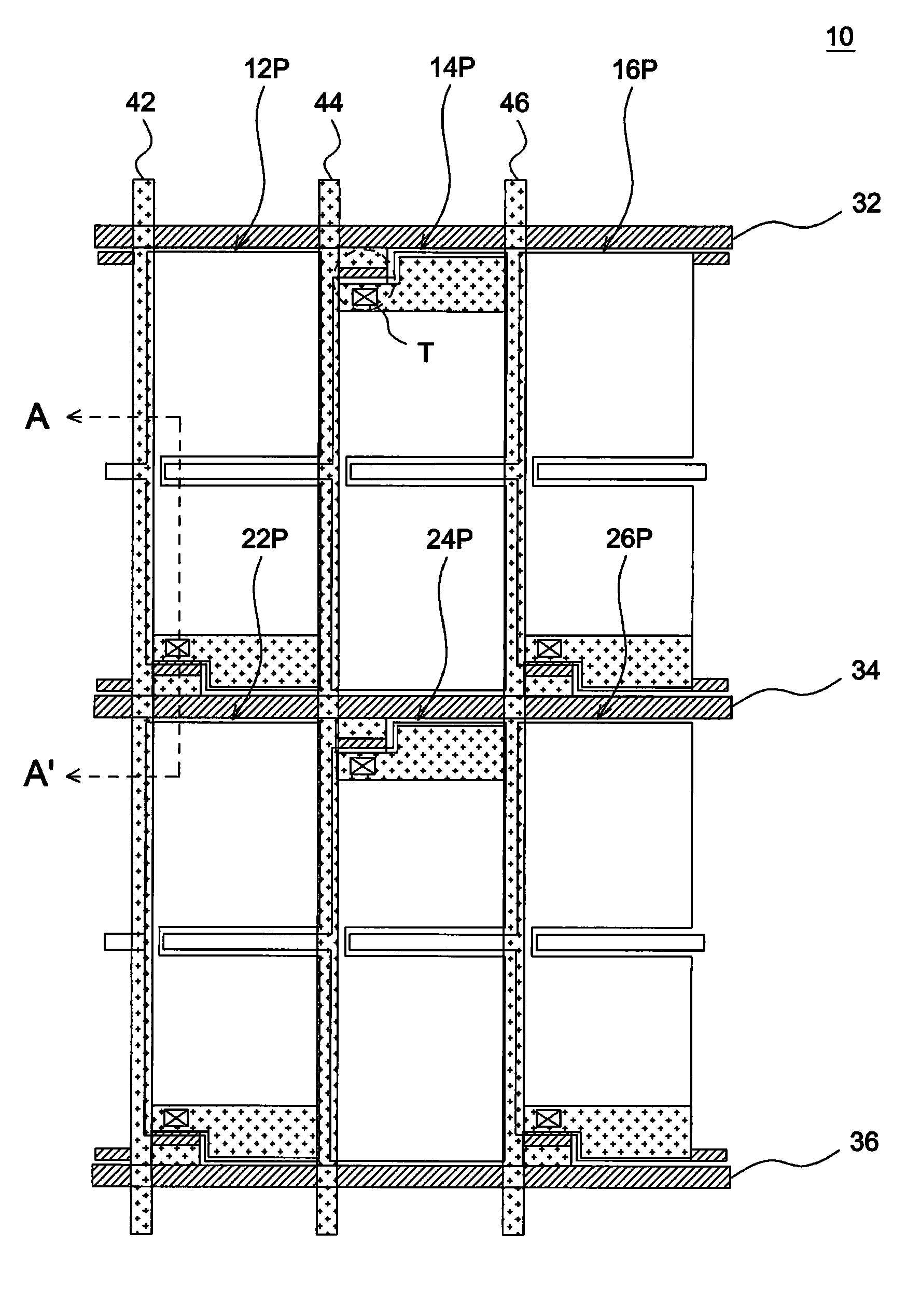
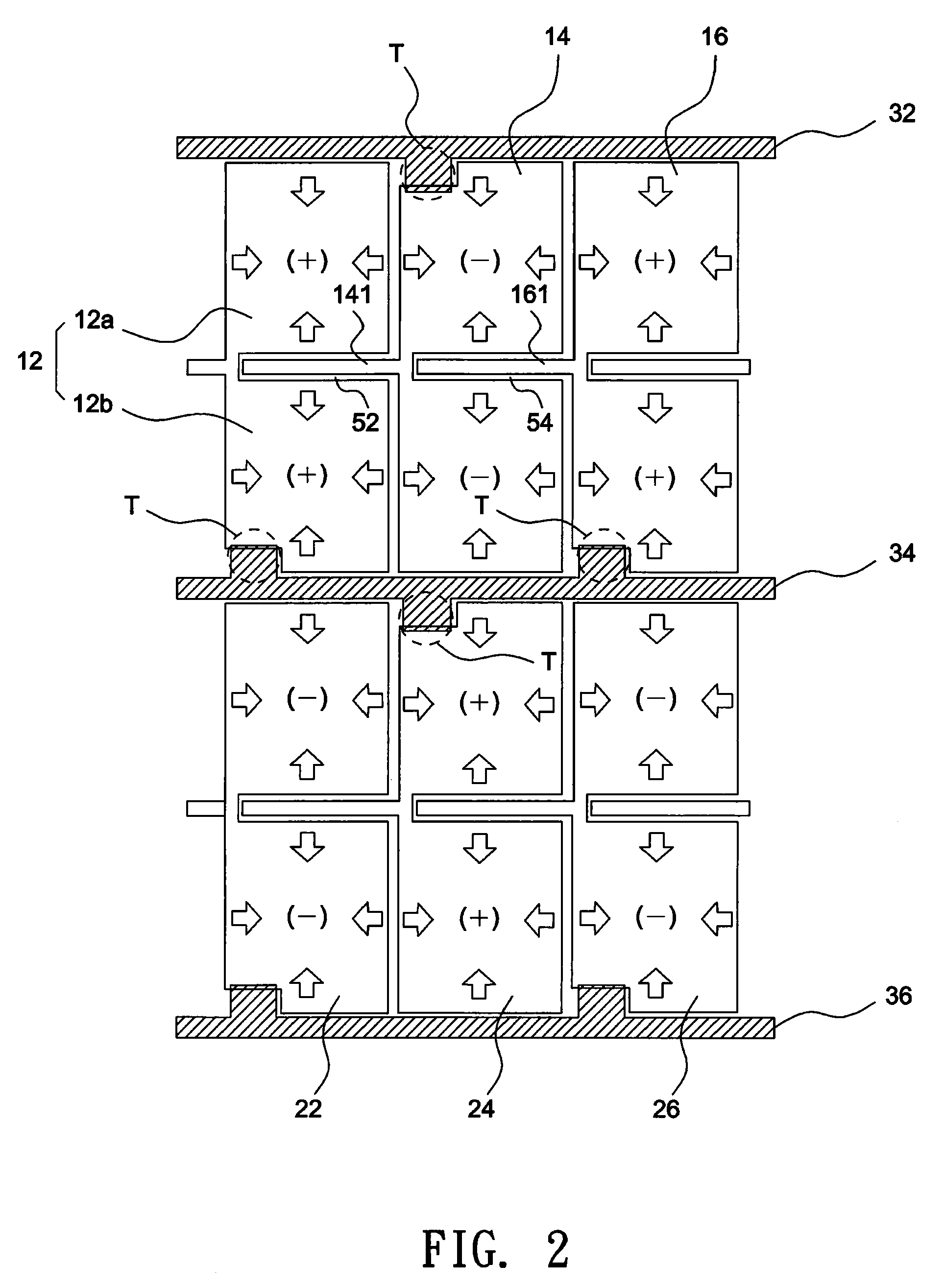
[0022]In the following detailed description of the preferred embodiments, reference is made to the accompanying drawings which form a part hereof, and in which are shown by way of illustration specific embodiments in which the invention may be practiced. In this regard, directional terminology is used with reference to the orientation of the Figure(s) being described. The components of the present invention can be positioned in a number of different orientations. As such, the directional terminology is used for purposes of illustration and is in no way limiting. On the other hand, the drawings are only schematic and the sizes of components may be exaggerated for clarity. It is to be understood that other embodiments may be utilized and structural changes may be made without departing from the scope of the present invention. Also, it is to be understood that the phraseology and terminology used herein are for the purpose of description and should not be regarded as limiting. The use ...


PUM

PropertyMeasurementUnit
distribution areaaaaaaaaaaa
areaaaaaaaaaaa
polarityaaaaaaaaaa

Abstract

A thin film transistor array substrate includes an insulating substrate, a plurality of scan lines, an insulating layer, a plurality of data lines, and a plurality of pixels arranged in an array of rows and columns. The pixels in each row are aligned in a row direction, the pixels in each column are aligned in a column direction, and the pixels are separated from each other by the scan lines and the data lines. Each pixel includes a thin film transistor and a pixel electrode. The pixel electrode has at least one opening that extends from the periphery to the inside of the pixel electrode and at least one extension part that extends in the row direction into an opening of a neighboring pixel electrode in the same row. Each of the scan lines alternately controls one of the pixel electrodes in a first row and one of the pixel electrodes in a second row immediately adjacent to the first row.

Description

CROSS REFERENCE TO RELATED APPLICATION[0001]This application claims priority of application No. 096147824 filed in Taiwan R.O.C on Dec. 14, 2007 under 35 U.S.C. §119; the entire contents of which are hereby incorporated by reference.FIELD OF THE INVENTION[0002]The invention relates to a thin film transistor (TFT) array substrate.DESCRIPTION OF THE RELATED ART[0003]Typically, the display contrast ratio and response speed offered by a VA (vertically-aligned) mode liquid crystal display, which uses negative liquid crystal materials and vertical alignment films, are better than a TN (twisted-nematic) mode LCD, since liquid crystal molecules are aligned in a vertical direction when no voltage is applied. Also, it is known the viewing angle performance of a VA mode LCD is improved by setting the orientation directions of the liquid crystal molecules inside each picture element to a plurality of mutually different directions; that is, forming multiple distinct domains in the liquid crystal...

Claims


Application Information

Patent Timeline
Patent Type & Authority Patents(United States)
IPC IPC(8): G02F1/141G02F1/1343
CPCG02F1/133707G09G3/3648G02F1/134336G09G3/3614H01L27/124G09G2300/0439G09G2300/0447G09G2320/028G09G2330/021G09G2300/0426
Inventor WANG, WEN-CHUNLIU, CHIN-CHANGWANG, I FANG
Owner WINTEK CORP
Why Eureka
Try Eureka