On-chip embedded thermal antenna for chip cooling

a technology of thermal antenna and chip, which is applied in the field of semiconductor chips, can solve the problems of complicated further, affecting and the influence of k dielectric materials on the dissipation of heat generated by the integrated circuit wir

Active Publication Date: 2011-11-08
GLOBALFOUNDRIES US INC
View PDF6 Cites 42 Cited by
  • Summary
  • Abstract
  • Description
  • Claims
  • Application Information

AI Technical Summary

Problems solved by technology

Such low-K dielectric materials also impact dissipating heat generated by the integrated circuit wires themselves.
This problem is complicated further by stacked chip effort of today's advanced devices.

Method used


Image

  • On-chip embedded thermal antenna for chip cooling
  • On-chip embedded thermal antenna for chip cooling
  • On-chip embedded thermal antenna for chip cooling

Examples


Embodiment Construction

[0023]The embodiments of the invention and the various features and advantageous details thereof are explained more fully with reference to the non-limiting embodiments that are illustrated in the accompanying drawings and detailed in the following description.

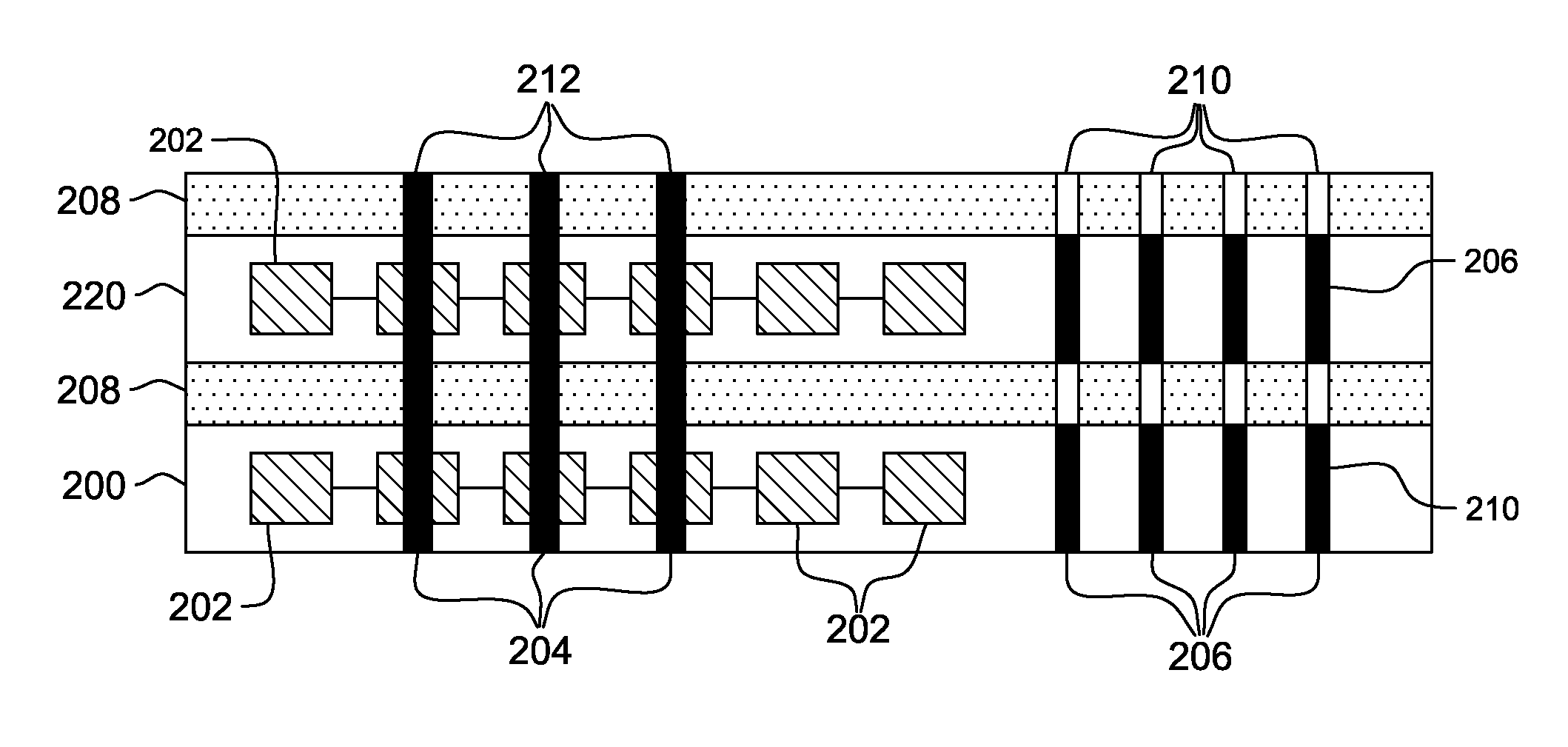
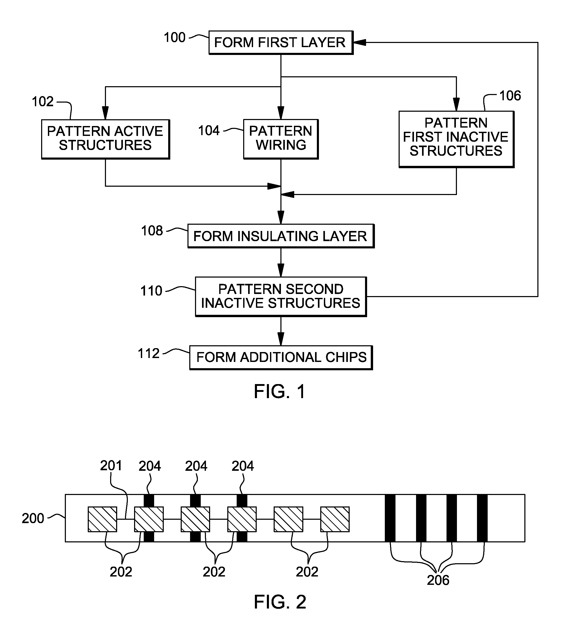
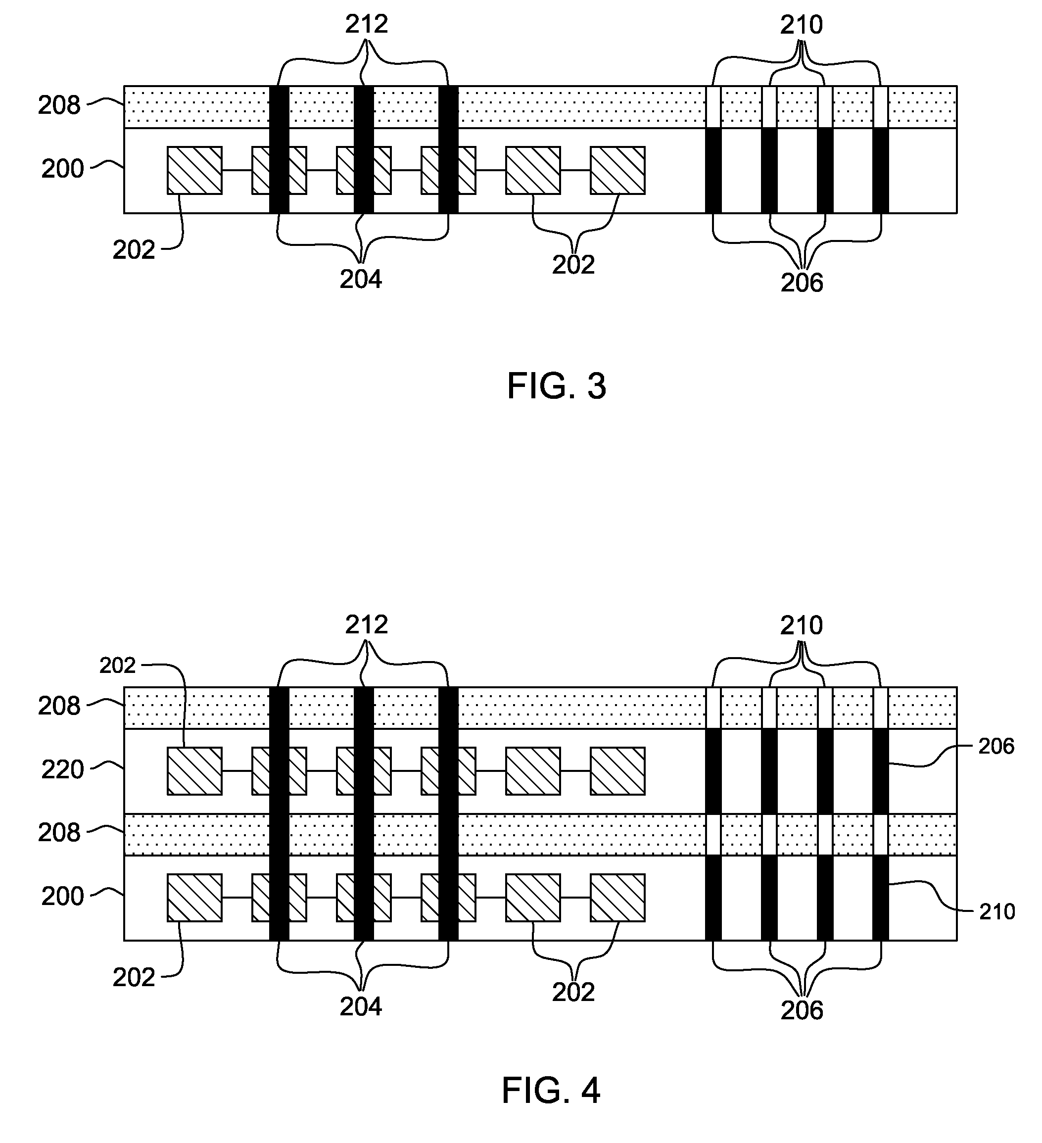
[0024]As mentioned above, the use of low-K dielectrics has increased the difficulty of transferring and dissipating heat generated by the active structures and wiring within an integrated circuit chip. Inactive (“dummy”) metallic fill structures are commonly used to minimize the topographical variation for polishing processes (chemical mechanical polishing CMP). Because such inactive structures are electrically and thermally conductive, they tend to increase the thermal conductivity of the structure, but it also increases the electrical noise within the chip. In other words, even though the inactive structures are electrically isolated from the wiring and active structures within the integrated circuit chip, because they are f...


PUM


Abstract

An apparatus comprises a first layer within a semiconductor chip having active structures electrically connected to other active structures and having electrically isolated first inactive structures. A second layer within the semiconductor chip is physically connected to the first layer. The second layer comprises an insulator and has second inactive structures. The first inactive structures are physically aligned with the second inactive structures.

Description

BACKGROUND[0001]1. Field of the Invention[0002]The embodiments of the invention generally relate to semiconductor chips and, more specifically, to semiconductor chips that include inactive devices that are aligned with each other to form a thermal path through the layers of the semiconductor chip and potentially through the entire semiconductor chip.[0003]2. Description of the Related Art[0004]Low dielectric constant materials (low-k dielectric materials) in multilevel very large scale integration (VLSI) circuits significantly decrease heat transfer. This inhibits heat generated by active devices from being able to travel through the back end metallurgies of a semiconductor chip to a heat sink at the top of the chip. Such low-K dielectric materials also impact dissipating heat generated by the integrated circuit wires themselves. This problem is complicated further by stacked chip effort of today's advanced devices. The joule heating of interconnect wires and vias can also be a majo...

Claims


Application Information

Patent Timeline
Patent Type & Authority Patents(United States)
IPC IPC(8): H01L23/52
CPCH01L23/3677H01L23/585H01L25/0657H01L25/50H01L2225/06513H01L2225/06541H01L2924/0002H01L2924/00
Inventor CHEN, FENGAMBINO, JEFFREY P.STRONG, ALVIN W.
Owner GLOBALFOUNDRIES US INC
Why Eureka
Try Eureka