

Digital wound detection system
a detection system and digital technology, applied in the direction of inter-force acceleration measurement, force/torque/work measurement apparatus, instruments, etc., can solve the problems of traumatic brain injury diagnosis, heavy and bulky devices are not generally available near battlefields, etc., and achieve the effect of diagnosing the severity of the injury
- Summary
- Abstract
- Description
- Claims
- Application Information
AI Technical Summary
Benefits of technology
Problems solved by technology
Method used
Image

Examples
exemplary embodiment 10
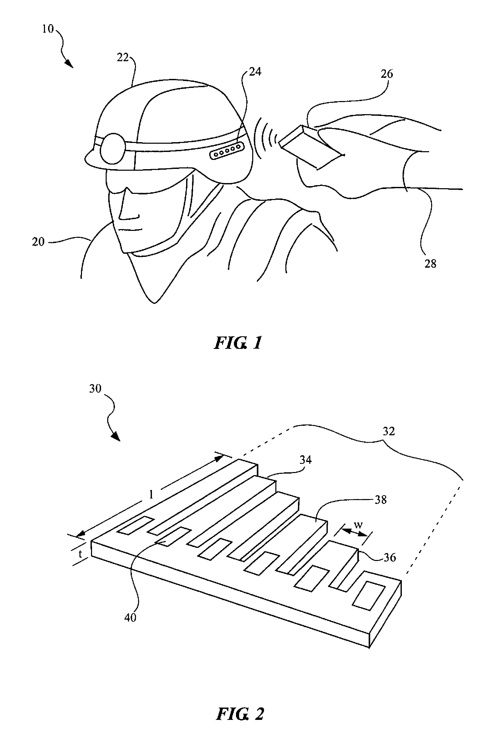
[0018]Illustrated in FIG. 1 is a schematic drawing of an exemplary embodiment 10 of the digital wound detection system as applied in a battlefield environment. The detection system of the present invention can comprise, among other things, an ultra-low power impact recorder capable of detecting, quantifying, recording and transmitting the maximum energy of a blast or impact to the head for aiding in the triage and diagnosis of Traumatic Brain Injury (TBI) in soldiers on the battlefield.
[0019]The embodiment 10 of the present invention can include a combat soldier 20 wearing a helmet 22, to which is attached a impact recorder 24 that can detect, quantify, and record the maximum value or absolute magnitude of a shock experienced by the head of the soldier, in response to the impact of a projectile or a shock wave from a nearly explosion. As can be appreciated, multiple impact recorders can be worn on the outside of the helmet, on the inside webbing, or on a headband or covering placed ...
exemplary embodiment 100
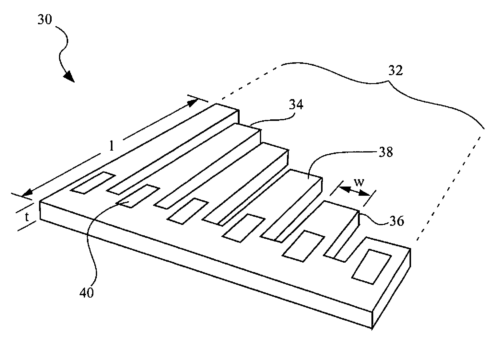
[0044]Illustrated in FIG. 5 is a perspective, cut-away view of the digital wound detection system, according to an exemplary embodiment 100 of the present invention. This embodiment can include a self-powered shock sensor 110 configured to self-generate an electric signal proportional to the shock value of the ballistic impact, an electronic circuit 130 configured to carry the electric signal away from the shock sensor, and a latchable electronic memory 150 that is configured to capture the maximum value of the electric signal proportional to the shock value of a ballistic impact.
[0045]The shock sensor 110 can be fabricated using a thin-film piezoelectric deposition process and standard semiconductor fabrication techniques to form a thin film piezoelectric microcantilever. As shown in FIG. 5, a silicon wafer 102 can be covered with a plurality of surface layers 104, 106 which, for the purposes of this detailed description, can be representative of a plurality of sub-layers including...
PUM
| Property | Measurement | Unit |
|---|---|---|
| frequencies | aaaaa | aaaaa |
| frequency | aaaaa | aaaaa |
| frequencies | aaaaa | aaaaa |
Abstract
Description
Claims
Application Information