Bonding method of dissimilar materials made from metals and bonding structure thereof
a technology of dissimilar materials and bonding structure, which is applied in the direction of manufacturing tools, welding/soldering/cutting articles, transportation and packaging, etc., can solve the problems of increasing weight or cost, inability to obtain sufficient seam strength, and weakening of bonded portions
- Summary
- Abstract
- Description
- Claims
- Application Information
AI Technical Summary
Benefits of technology
Problems solved by technology
Method used
Image
Examples
fifth embodiment
[0019]FIGS. 6A and B are cross-sectional explanatory views of a bonding process of a three-sheet bundle using a bare steel plate of a fifth embodiment; and
sixth embodiment
[0020]FIGS. 7A and B are cross-sectional explanatory views of a bonding process of a four-sheet bundle.
DETAILED DESCRIPTION OF EMBODIMENTS OF THE INVENTION
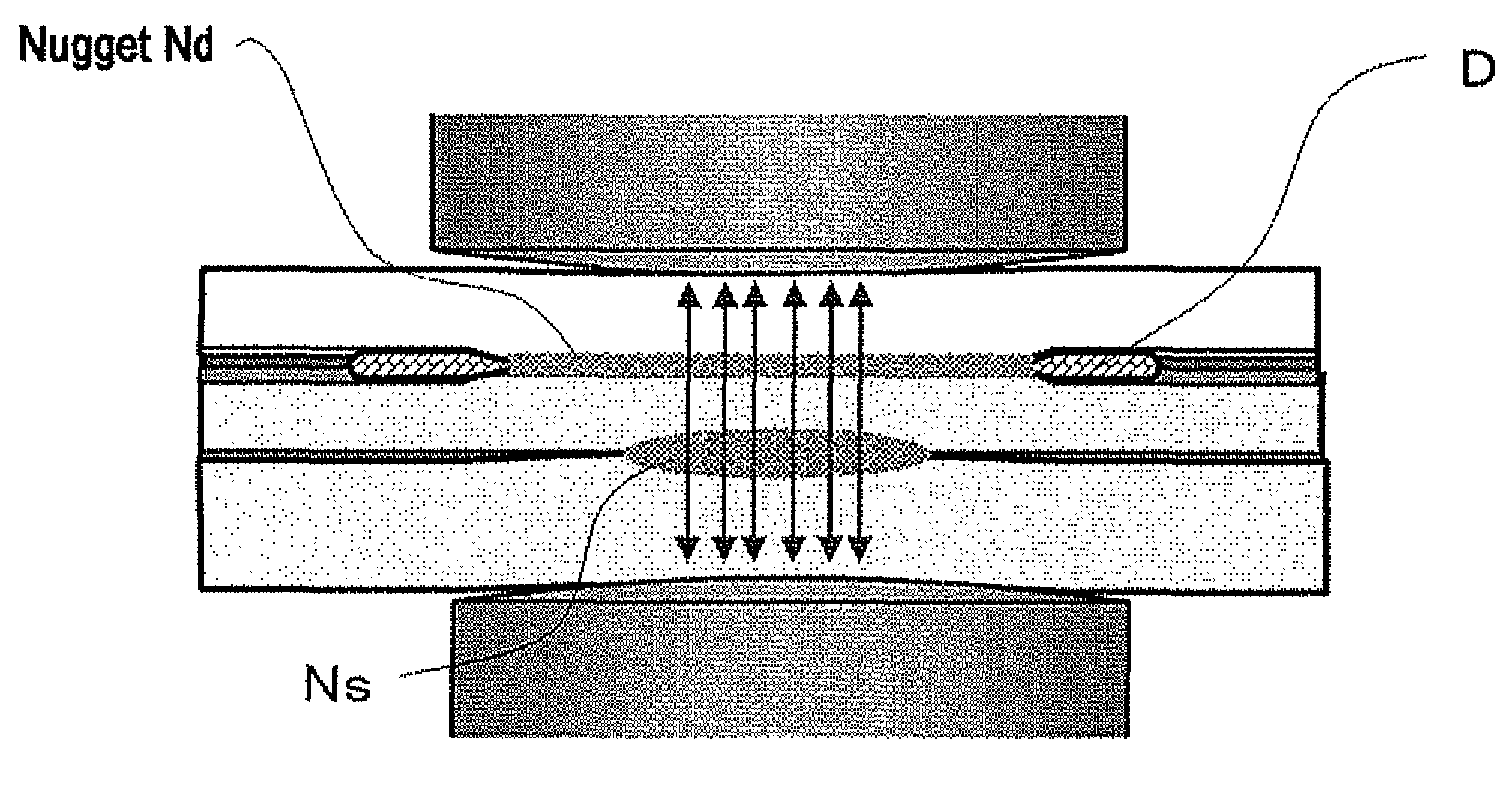
[0021]Bonding methods disclosed herein are capable of sufficiently securing the bonding strength in each of the interfaces, wherein a desired nugget diameter can be formed in each interface while inhibiting a decrease in thickness of the material at a low melting point side. The methods can be utilized when three or more sheets of dissimilar materials made from metals are layered and bonded by the resistance welding operation. The methods can also be utilized for a combination of the materials that has both the same material interface and the dissimilar material interface and in which a resistance heating in the dissimilar material interface becomes smaller than that in the same material interface due to the contact resistance difference between both interfaces. Also disclosed is a bonding structure obtained by such bonding method...
first embodiment
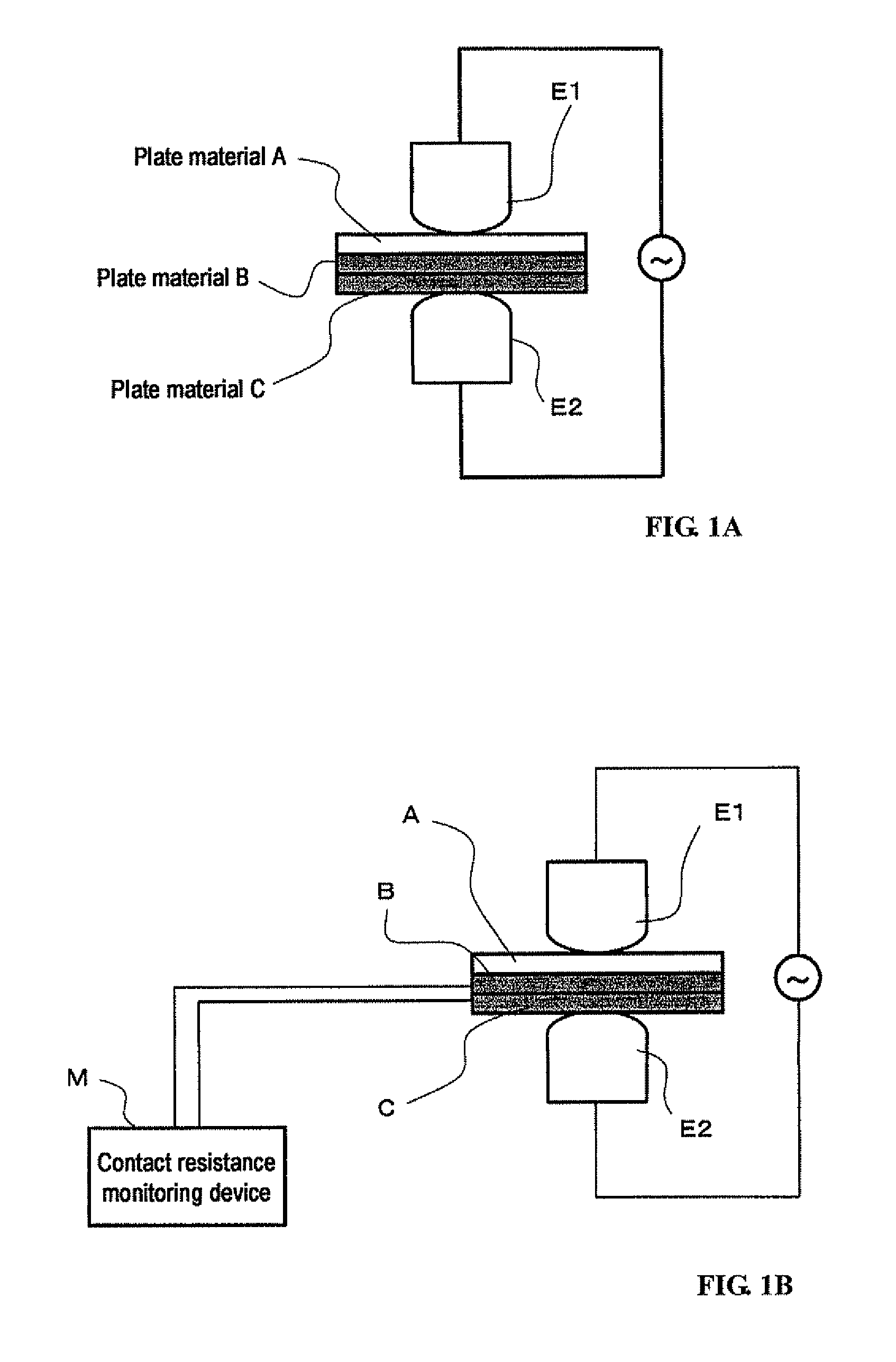
[0056]A first embodiment as depicted in FIGS. 4A and 4B is next described. As shown in FIG. 4A, a bonding operation of a three-sheet bundle is performed wherein a 6000 system aluminum alloy plate 1 having a thickness of 1.0 mm, a zinc plated steel plate 2 having a thickness of 0.8 mm and a bare steel plate 3 having a thickness of 1.2 mm are layered in that order. A spot welding device of an AC power type having a contact resistance monitoring device as shown in FIG. 1B is used along with an R-type electrode having a radius of curvature of a leading end curved surface of 40 mm as the electrodes E1 and E2.
[0057]To form the nugget Ns in the same material interface (i.e., the interface between the zinc plated steel plate 2 and the bare steel plate 3), a pressing force of 300 kgf is applied and an AC current of 4000 A is conducted while continuously monitoring the contact resistance of the same material interface with monitoring device M. When the contact resistance of the same material ...
PUM
| Property | Measurement | Unit |
|---|---|---|
| current conducting time | aaaaa | aaaaa |
| thickness | aaaaa | aaaaa |
| temperature | aaaaa | aaaaa |
Abstract
Description
Claims
Application Information


