Signal processing device and method

a signal processing and signal technology, applied in the direction of amplitude demodulation, dc level restoring means or bias distort correction, baseband system details, etc., can solve the problems of deteriorating the evm (error vector magnitude: modulation accuracy) of the radio frequency signal, and affecting the transmission quality. , to achieve the effect of reducing carrier leakage, simple configuration, and excellent communication quality

Active Publication Date: 2011-11-15
NEC CORP
View PDF28 Cites 1 Cited by
  • Summary
  • Abstract
  • Description
  • Claims
  • Application Information

AI Technical Summary

Benefits of technology

[0020]Thus, it is an object of the present invention to provide a signal processing device and method that can detect the DC shift component without using a spectrum analyzer or a power amplifier for detection.
[0021]Also, it is another object of the invention to provide a signal processing device and method that can correct the detected DC shift component.
[0024]Also, in this invention, an offset correction signal for making a level difference between the detected positive signal and the detected negative signal within a preset permissible range is generated, based on the comparison result of the level comparator, and the offset of the modulated signal supplied from the outside is corrected in accordance with the offset correction signal. Therefore, the DC shift component of the modulated signal can be corrected with a simple configuration. Accordingly, it is possible to obtain a communication system that has excellent communication quality in which there is reduced carrier leakage in the transmitted signal by using the signal processing device of the invention.

Problems solved by technology

When the carrier leak occurs, the signal waveform of the radio frequency signal outputted from the mixer is deviated from the ideal waveform, deteriorating the EVM (Error Vector Magnitude: Modulation Accuracy) of the radio frequency signal.
It is well known that such carrier leaks caused by the DC shift component deteriorates the EVM of the radio frequency signal used in the communication system and degrades the communication quality, as described above.
It is well known that the carrier leak is similarly caused by the DC shift component in the circuits such as a power amplifier, a phase converter and a frequency selector, for example, other than the mixer provided for the signal processing device, whereby the carrier leak caused by the DC shift component in the circuits other than the mixer also degrades the communication quality.
However, there is a problem that the wave detector circuit can only correctly detect a signal having a certain power or more due to fluctuating circuit parameters.
In particular, when the power of the radio frequency signal is detected, a power amplifier for a high frequency signal is required, resulting in a problem that the configuration of the detection circuit becomes complex.
Also, if the detection circuit is provided with the high gain power amplifier for a high frequency signal, there is a problem that the circuit scale will become larger, and the power consumption will increase.

Method used


Image

  • Signal processing device and method
  • Signal processing device and method
  • Signal processing device and method

Examples


first exemplary embodiment

[0123]A first example of the signal processing device according to the invention will be described below with reference to the drawings.

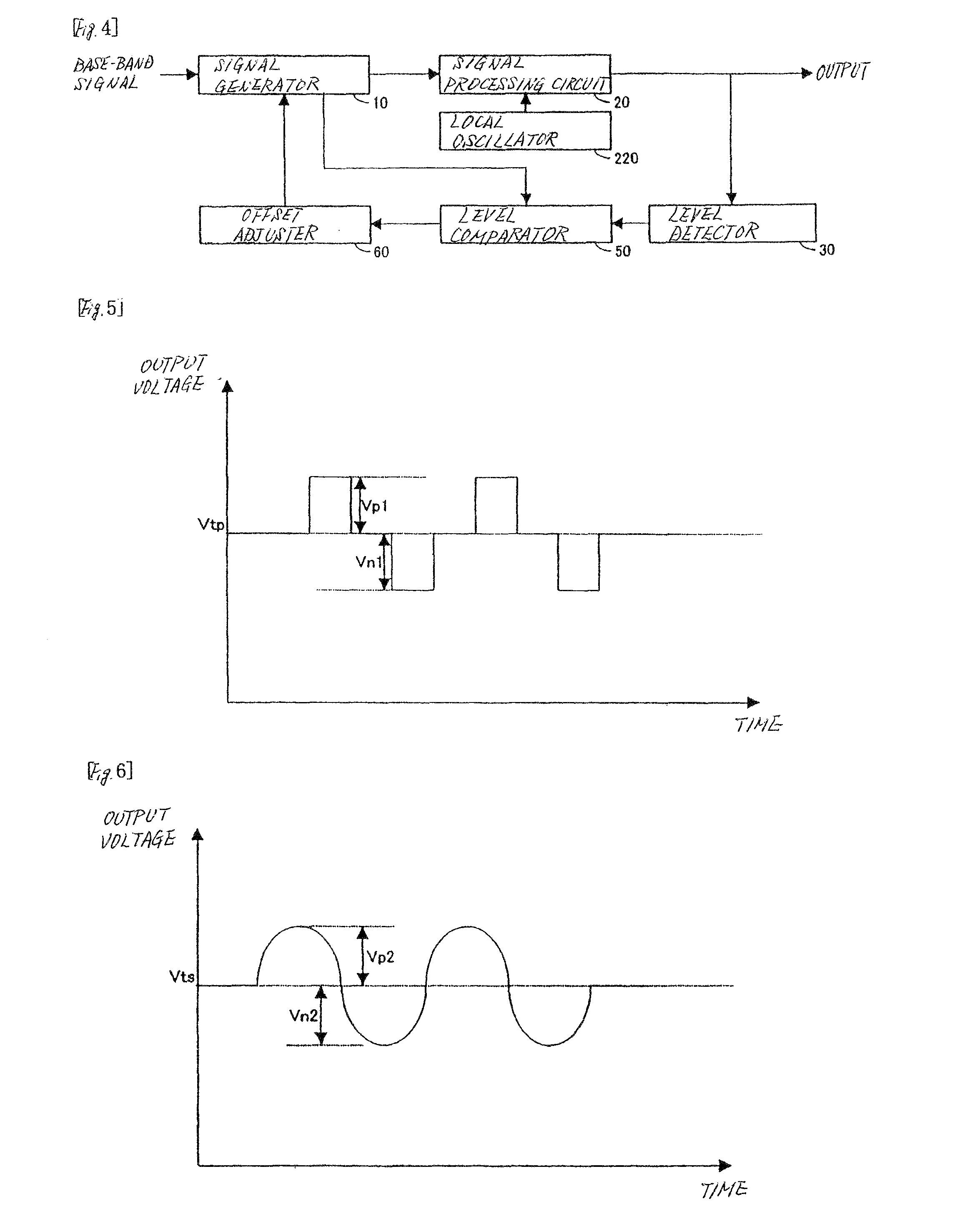
[0124]An example of signal generator 10 as shown in FIG. 4 is shown in the first exemplary embodiment.

[0125]Signal generator 10 comprises signal source 110 for generating the test signal in which the amplitude in the positive direction and the amplitude in the negative direction are equal with respect to the reference voltage, condenser 120 for removing the DC component of the test signal, and coil 130 for superimposing the offset correction signal on the test signal, as shown in FIG. 20.

[0126]FIG. 20 only shows a function for generating the test signal, which signal generator 10 has, but if signal source 110 as shown in FIG. 20 is replaced with a terminal for inputting the modulated signal (base-band signal) supplied from the outside, a circuit for processing the modulated signal (base-band signal) is available.

[0127]From the test signal outputted ...

second exemplary embodiment

[0129]A second exemplary embodiment of the signal processing device according to the invention will be described below with reference to the drawings.

[0130]An example of level comparator 50 as shown in FIG. 4 is shown in the second exemplary embodiment.

[0131]Level comparator 50 of this exemplary embodiment comprises positive signal level holding part 2810 for holding the detection level of the detected positive signal outputted from level detector 30, negative signal level holding part 2815 for holding the detection level of the detected negative signal outputted from level detector 30, and difference signal output part 2820 for outputting the comparison result of comparing the detection levels outputted from positive signal level holding part 2810 and negative signal level holding part 2815, as shown in FIG. 21.

[0132]Positive signal level holding part 2810 adopts in the level of the detected positive signal (e.g., detection level DPT4 of the detected positive signal DP4 as shown in...

third exemplary embodiment

[0140]A third exemplary embodiment of the signal processing device according to the invention will be described below with reference to the drawings.

[0141]A specific example of level comparator 50 as shown in the second exemplary embodiment is shown in the third exemplary embodiment.

[0142]Level comparator 50 of this exemplary embodiment comprises first sample / hold circuit 3110 for holding and outputting the detection level of the detected positive signal outputted from level detector 30, second sample / hold circuit 3115 for holding and outputting the detection level of the detected negative signal outputted from level detector 30, and comparator 3120 for comparing the detection levels outputted from first sample / hold circuit 3110 and second sample / hold circuit 3115 to output the comparison result, as shown in FIG. 22.

[0143]First sample / hold circuit 3110 adopts in the level of the detected positive signal (e.g., detection level DPT4 of detected positive signal DP4 as shown in FIG. 11)...


PUM


Abstract

A test signal is generated and supplied to a signal processing circuit for making frequency conversion. A signal outputted from the signal processing circuit is detected to generate a detected signal including a detected positive signal corresponding to the positive signal of the test signal and a detected negative signal corresponding to the negative signal. And the level of the detected positive signal and the level of the detected negative signal are compared to output the comparison result indicating which level is higher. Further, an offset correction signal for making a level difference between the detected positive signal and the detected negative signal within a preset permissible range is generated, based on the comparison result, and offset correction of the test signal or modulated signal supplied from the outside is made in accordance with the offset correction signal.

Description

TECHNICAL FIELD[0001]The present invention relates to a signal processing device and method for correcting a DC shift component of a high frequency signal.BACKGROUND ART[0002]In a transmitter provided for a communication system or communication terminal, a base-band signal including user data is converted into a radio frequency signal by a signal processing device having a mixer and a power amplifier, and transmitted after amplifying the signal power, as needed.[0003]Herein, if a DC (Direct Current) shift component exists in the base-band signal inputted into the mixer, the mixer outputs a radio frequency (RF: Radio Frequency) signal including a carrier leak caused by the DC shift component.[0004]When the carrier leak occurs, the signal waveform of the radio frequency signal outputted from the mixer is deviated from the ideal waveform, deteriorating the EVM (Error Vector Magnitude: Modulation Accuracy) of the radio frequency signal.[0005]Therefore, a spectrum analyzer was convention...

Claims


Application Information

Patent Timeline
Patent Type & Authority Patents(United States)
IPC IPC(8): H04L25/06
CPCH04B1/0475H04L1/24H04L1/244H04L27/368
Inventor YANAGISAWA, KIYOSHIMATSUNO, NORIAKI
Owner NEC CORP
Why Eureka
Try Eureka