
Photonic detector, imaging system and method employing plasmonic resonance absorption

a plasmonic resonance absorption and photonic detector technology, applied in the field of photonic detectors, can solve the problems of ir imaging systems that employ these semiconductor-based ir photonic detectors that are not typically able to be used, and many imaging systems based on semiconductor photodiodes are limited to a finite number of spectral bands

Active Publication Date: 2011-11-29
HRL LAB
View PDF5 Cites 6 Cited by
  • Summary
  • Abstract
  • Description
  • Claims
  • Application Information

AI Technical Summary

Problems solved by technology

Unfortunately, the existing photonic detectors often fail to meet one or more objectives of many modern imaging systems that cover the visible to LWIR spectrum.
As such, IR imaging systems that employ these semiconductor-based IR photonic detectors are not typically able to be used when room-temperature operation is desired unless an associated cost, complexity and power consumption for sensor cooling can be accommodated.
In addition, many imaging systems based on semiconductor photodiodes are limited to a finite number of spectral bands due to the material bandgaps used in such devices.
However, microbolometer arrays generally exhibit spectral sensitivity that is limited to the LWIR spectrum which may preclude their use in some multi-spectral imaging applications.
Furthermore, in general the above-discussed photonic detectors typically lack an integrated ability to achieve wavelength tunability.

Method used


Image

  • Photonic detector, imaging system and method employing plasmonic resonance absorption
  • Photonic detector, imaging system and method employing plasmonic resonance absorption
  • Photonic detector, imaging system and method employing plasmonic resonance absorption

Examples


Embodiment Construction

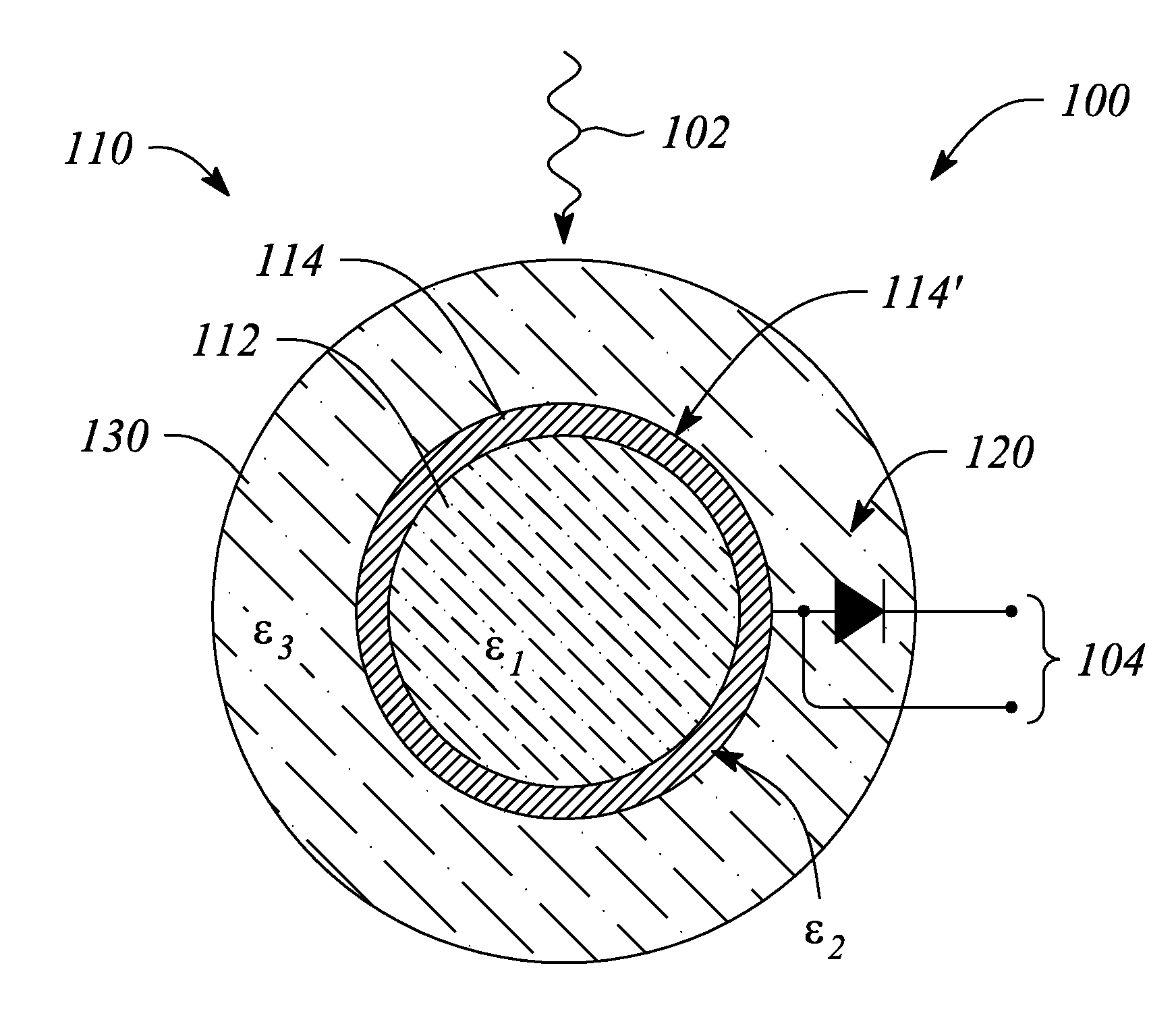
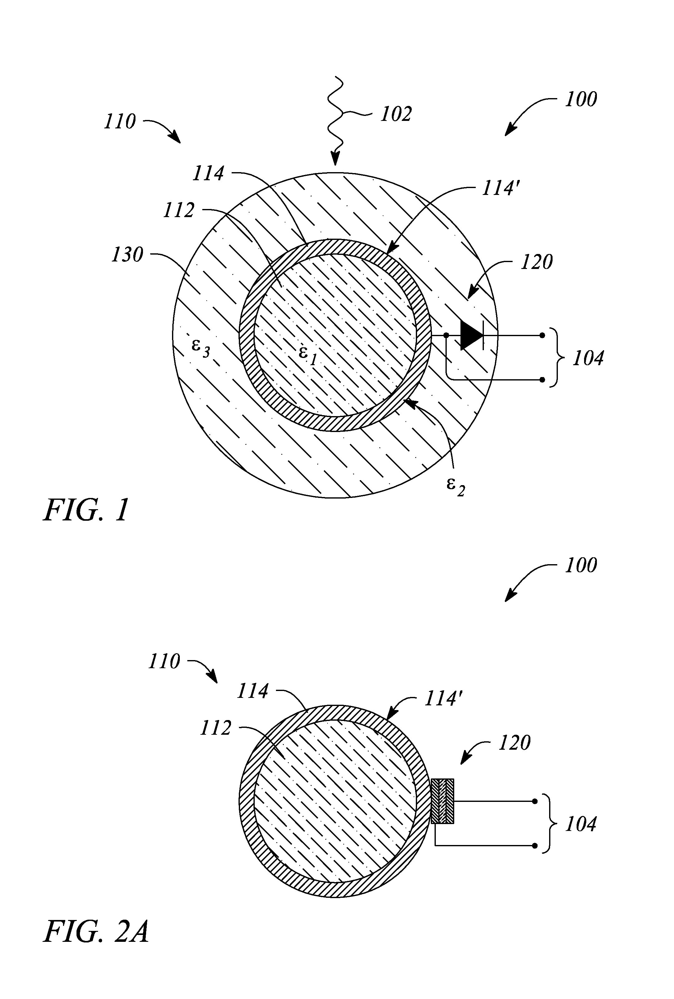
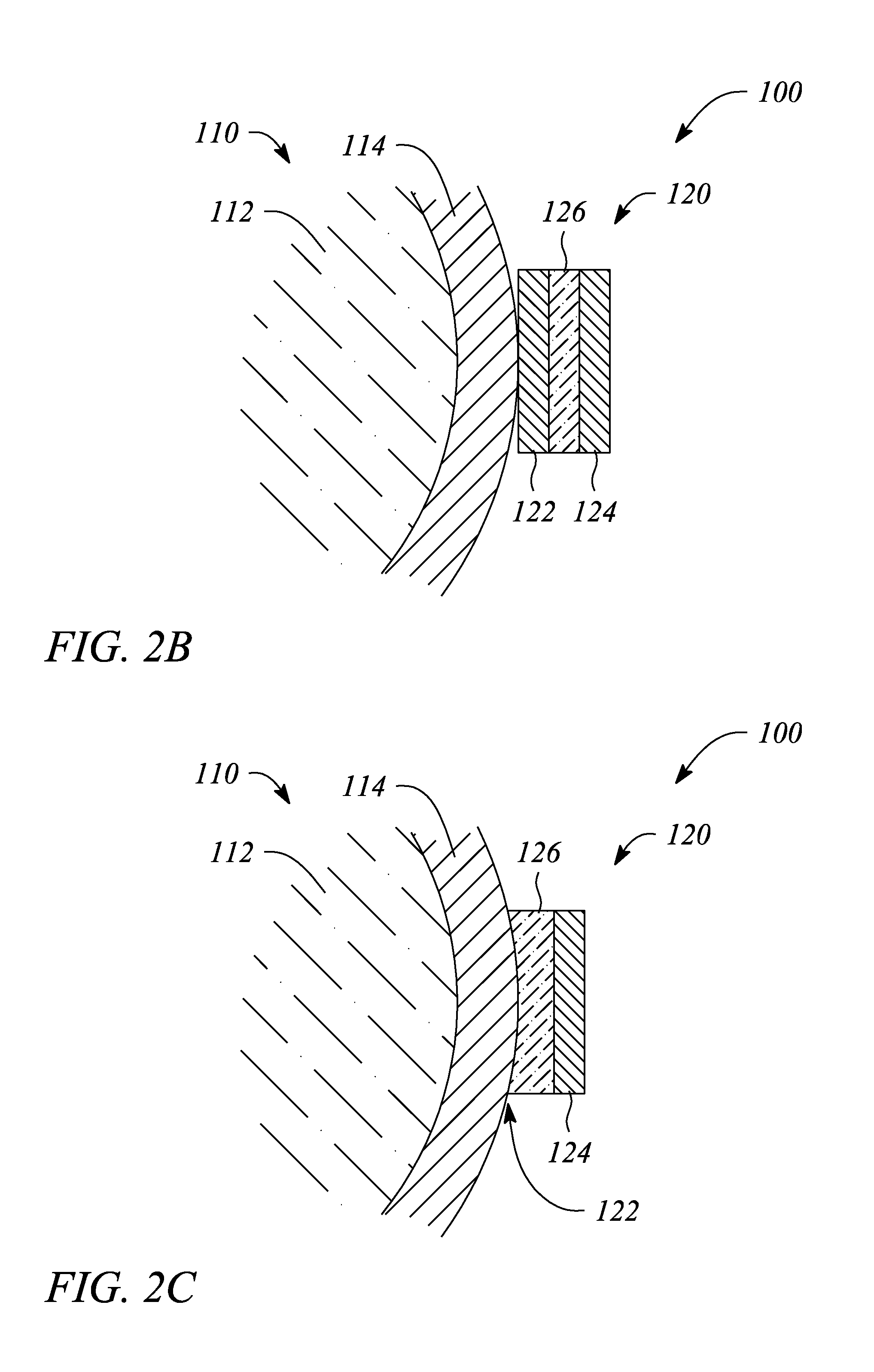
[0023]Embodiments of the present invention facilitate detection of optical signals (i.e., photonic detection) using plasmonic resonant absorption. In particular, according to various embodiments of the present invention, plasmonic resonant absorption (PRA) is employed to absorb electromagnetic (EM) radiation of an incident optical signal. The PRA absorbed EM radiation is converted into or excites a surface plasmon. The excited surface plasmon has associated with it a relatively strong evanescent electric field which is rectified to produce a direct current (DC) signal. The DC signal produced by rectifying the evanescent field associated with the surface plasmon is proportional to, and thus effectively provides detection of, the incident optical signal. As such, the present invention provides PRA-based photonic detection. Moreover, the photonic detection of the present invention exhibits high sensitivity as a result of the relatively strong evanescent electric field produced through ...


PUM

PropertyMeasurementUnit
Dielectric polarization enthalpyaaaaaaaaaa
Electric potential / voltageaaaaaaaaaa
Wavelengthaaaaaaaaaa

Abstract

A photonic detector, a photonic imaging system and a method of photonic detection employ plasmonic resonant absorption to detect an incident electromagnetic signal. The photonic detector and imaging system include a micro / nanoshell (MNS) structure that supports a surface plasmon and a rectifying junction that rectifies an evanescent electric field of the surface plasmon. The surface plasmon is excited by the incident electromagnetic signal at a plasmonic resonant absorption wavelength of the MNS structure. The method of photonic detection includes providing an MNS structure, exciting a surface plasmon on the MNS structure and rectifying an evanescent electric field of the excited surface plasmon to produce a rectified output signal. The rectified output signal provides detection of the incident electromagnetic signal.

Description

CROSS-REFERENCE TO RELATED APPLICATIONS[0001]N / ASTATEMENT REGARDING FEDERALLY SPONSORED RESEARCH OR DEVELOPMENT[0002]N / ABACKGROUND[0003]1. Technical Field[0004]The invention relates to photonic devices. In particular, the invention relates to photonic detectors that employ surface plasmons.[0005]2. Description of Related Art[0006]Photonic detectors or sensors of various types, employed either singly or in an array, are used in a wide variety of modern optical and infrared (IR) imaging systems. For example, modern digital photography depends almost exclusively on photonic sensor arrays that employ either charge-coupled devices (CCDs) or complementary metal oxide semiconductor (CMOS) active pixel sensors for capturing and creating digital images. Other photonic detection technologies are also often employed, especially in multispectral and hyperspectral imaging systems having operational imaging requirements that may extend well into the long-wave IR (LWIR) spectral range. These other...

Claims


Application Information

Patent Timeline
IPC IPC(8): G01J1/00B32B5/16
CPCB82Y20/00H04N5/335B82Y30/00Y10T428/2991H04N25/00
Inventor SAYYAH, KEYVAN
Owner HRL LAB
Learn More