

Variable feature interface that induces a balanced stress to prevent thin die warpage
a technology of feature interface and stress, which is applied in the field of manufacturing integrated circuits, can solve the problems of loss of time and resources, loss of structural strength of first die, and insufficient mechanical strength of thin die, and achieve the effect of preventing warpage during semiconductor assembly
- Summary
- Abstract
- Description
- Claims
- Application Information
AI Technical Summary
Benefits of technology
Problems solved by technology
Method used
Image

Examples
first embodiment
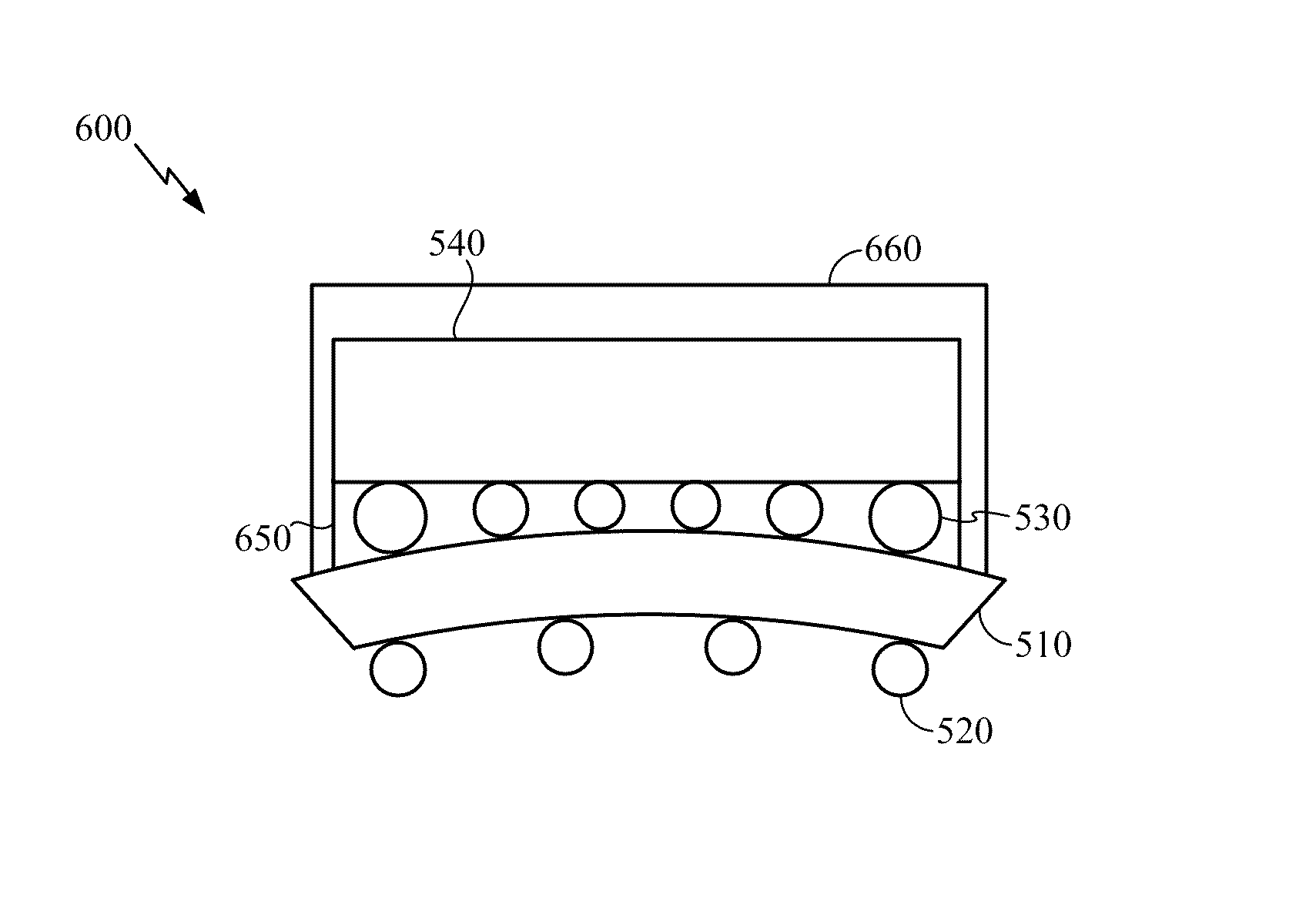
[0033]FIG. 5 is a block diagram illustrating an exemplary packaged die having induced reverse bending according to a A packaged die 500 includes a packaging substrate 510 having a packaging connection 520. Coupled to the packaging substrate 510 is a die 540. The die 540 is coupled to the packaging substrate 510 through an interconnect structure 530. The interconnect structure 530 may be, for example, bumps or pillars.
[0034]A reverse bending of the die 540 occurs during reflow of the interconnect structure 530 (and / or during compression of the die 540 towards the packaging substrate 510) by varying a height of the interconnect structure components (e.g., bumps or pillars). When the die 540 is compressed against the packaging substrate 510 the die 540 bends. Bending of the die 540 in one embodiment is designed to induce an inverse bend resulting from an inverse stress to counter bending imposed by a heating and cooling process such as reflow. A controlled inverse bend may be engineer...
second embodiment
[0044]Another example of balancing bending in a semiconductor die by inducing a reverse bending is now explained with reference to FIG. 7 and FIG. 8. FIG. 7 is a block diagram illustrating an exemplary packaged die having induced reverse bending according to a A packaged die 700 includes a packaging substrate 710 having a packaging connection 720. Coupled to the packaging substrate 710 is a die 740. The die 740 is coupled to the packaging substrate 710 through an interconnect structure 730. The interconnect structure 730 may be bumps of a ball grid array or solder pillars, for example.
[0045]A reverse bend may be induced through the interconnect structure 730 by varying a height of the interconnect structure 730 corresponding to location relative to the die 740. For example, if the interconnect structure 730 is bumps of a ball grid array, the height of each bump is varied. A bump 730A at the periphery of the die 740 is smaller than a bump 730B closer to the center of the die 740. Th...
PUM
 Abstract
Description
Claims
Application Information