Semiconductor device

a technology of semiconductor devices and semiconductor components, applied in semiconductor devices, semiconductor/solid-state device details, electrical apparatus, etc., can solve the problems of increasing the number of components that constitute semiconductor devices, difficult to reduce inductance, and complicated handling of components by workers, so as to reduce the inductance of low reduce the inductance of high-voltage bus bars and other circuit portions, and reduce the inductan

Inactive Publication Date: 2010-06-17
HONDA MOTOR CO LTD
View PDF3 Cites 54 Cited by
  • Summary
  • Abstract
  • Description
  • Claims
  • Application Information

AI Technical Summary

Benefits of technology

[0035]In this configuration, more current flows to the power semiconductor elements primarily when the motor is in power-running mode, but the portion of the bus bar from the high-voltage terminal to the power semiconductor element is lengthened, whereby the parallel portions are lengthened, and inductance can be farther reduced. The amount of current flowing to the rectifier semiconductor elements will increase during regeneration, field weakening, and the like, but inductance can be similarly reduced in these instances.
[0036]In the semiconductor-element module that is composed of the high-side and low-side semiconductor chips that constitute the bridge circuit of the inverter device in the configuration according to the first aspect of the present invention, the wiring pathway portion from the high-voltage terminal to the high-side semiconductor chip and the wiring pathway portion from that semiconductor chip to the output terminal are positioned in parallel and are configured so that the respective currents flow back and forth in opposite directions. The inductance of the high-voltage bus bar and other circuit portions can therefore be reduced. In the same semiconductor-element module, the wiring pathway portion from the output terminal to the low-side semiconductor chip and the wiring pathway portion from that semiconductor chip to the low-voltage terminal are positioned in parallel and are configured so that the respective currents flow back and forth in opposite directions. The inductance of the low-voltage bus bar and other circuit portions can therefore be reduced. Since the inductance can be reduced in the main circuit of the semiconductor-element module as described above, the switching loss and the surge voltage occurring during switching operations in the inverter device can be reduced.

Problems solved by technology

A problem is therefore presented in that reducing inductance is difficult when the configuration of the semiconductor device described in JP 2002-026251 A is applied to controlling a motor using the inverter device of a three-ph

Method used


Image

  • Semiconductor device
  • Semiconductor device
  • Semiconductor device

Examples


embodiment 1

[0061]The first embodiment of the semiconductor device according to the present invention will be described with reference to FIGS. 1 through 5.

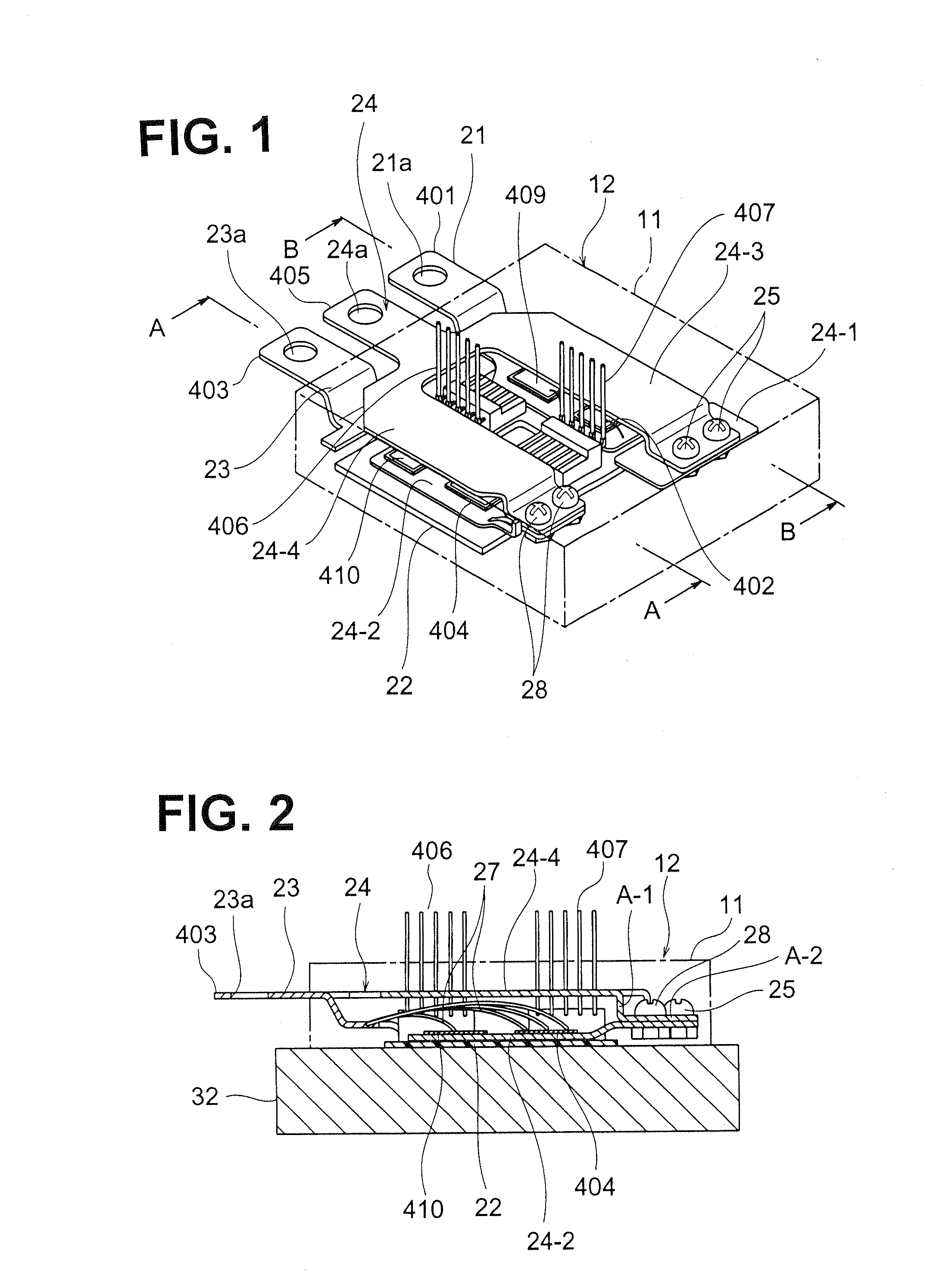
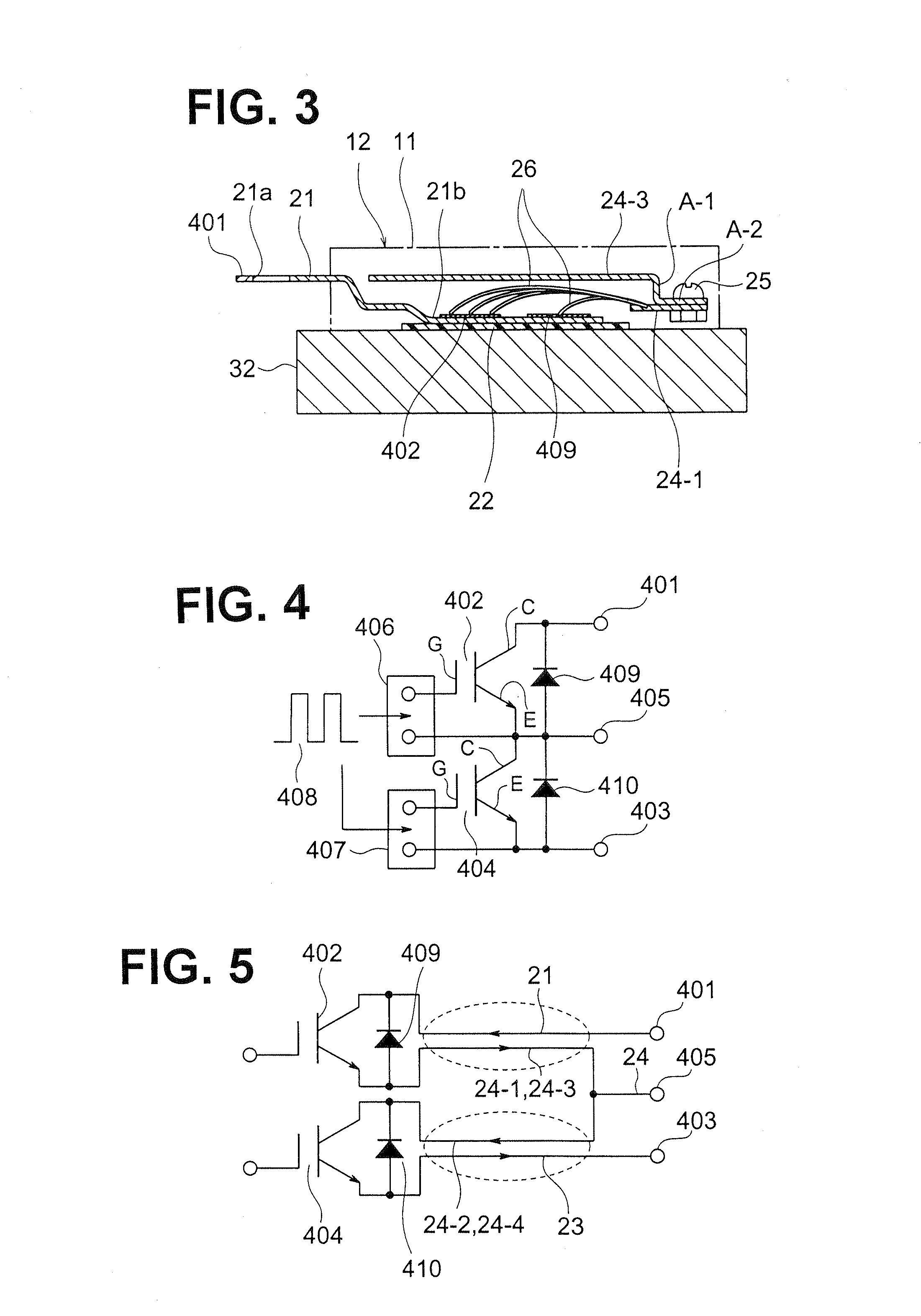
[0062]The semiconductor device described in the present embodiment is a power semiconductor device, and is typically an inverter device for driving a three-phase motor that drives an electric vehicle. The IGBT module shown in FIG. 1 displays the main portions of the inverter device. The configuration of the electrical circuit of the IGBT module will be described first with reference to FIG. 4.

[0063]FIG. 4 shows the electrical circuit portions of a single phase (one phase from among the U, V, or W phases) of the bridge circuit of the inverter device. The electrical circuit shown in FIG. 4 includes a high-side IGBT element 402 positioned near a high-voltage terminal 401 and a low-side IGBT element 404 positioned near a low-voltage terminal 403. The semiconductor elements used in the semiconductor device according to the present embodiment are ...

embodiment 2

[0102]A second embodiment of the semiconductor device of the present invention will be described next with reference to FIGS. 6 through 9.

[0103]The semiconductor device according to the second embodiment is a power semiconductor device that is an inverter device for driving a three-phase motor that drives a representative electric vehicle, as in the first embodiment. FIG. 6 is similar to the aforedescribed FIG. 1.

[0104]The configuration of the electrical circuit of the IGBT module according to the second embodiment is as was described using FIG. 4.

[0105]In other words, the electrical circuit portions of a single phase (one phase from among the U, V, or W phases) of the bridge circuit of the inverter device include the high-side IGBT element 402 positioned near the high-voltage terminal 401 and the low-side IGBT element 404 positioned near the low-voltage terminal 403. The bridge circuit of the inverter device is configured using six power semiconductor elements, but one module is fo...

embodiment 3

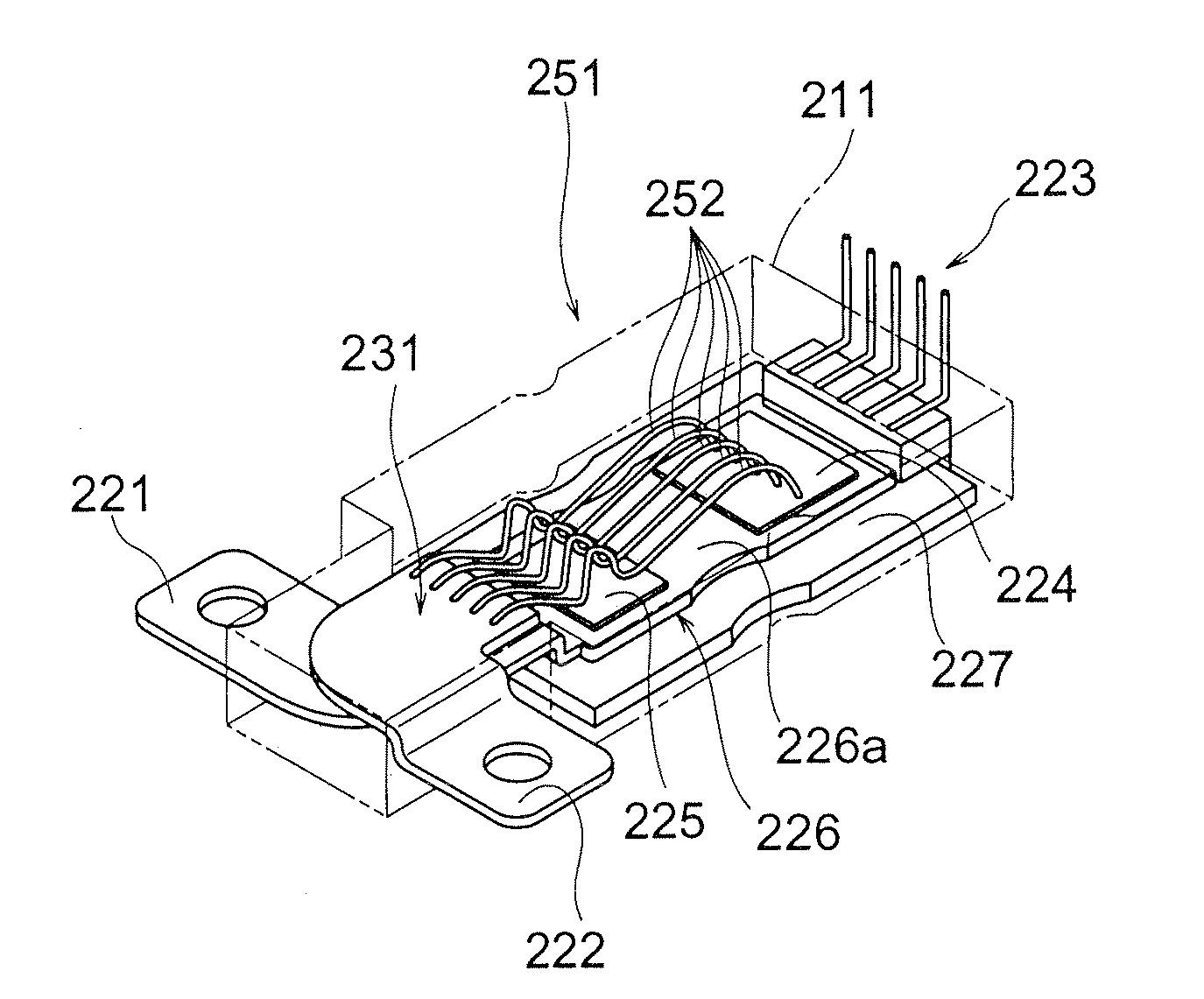
[0139]An embodiment of the basic configuration of a semiconductor device according to a third embodiment of the present invention will be described with reference to FIGS. 11 through 13. The semiconductor device according to the third embodiment is also used in an inverter device for driving a three-phase motor that drives an electric vehicle, like the previously described embodiments.

[0140]The physical structure of the IGBT will be described next with reference to FIGS. 11 through 13.

[0141]A block 211 shown by the alternatingly dotted line in FIGS. 11 and 12 designates the external shape of the package that forms an IGBT module 212. The block 211 is substantially molded from resin. The portions designated by solid lines in FIG. 11 are the physical structure portions of the wiring board. The resin mold 211 is shown by broken lines in FIGS. 11 and 12 and by a solid line in FIG. 13.

[0142]In FIG. 11, the portion designated by “221” is an input terminal, and the portion designated by “2...


PUM


Abstract

A semiconductor device is composed of a pair of semiconductor chips (402, 404) arranged parallel on the same flat plane; a high voltage bus bar (21) bonded on the surface on the collector side of one semiconductor chip (402); a low voltage bus bar (23) connected to the surface on the emitter side of the other semiconductor chip (404) with a bonding wire (27); a first metal wiring board (24-1) connected to the surface on the emitter side of the semiconductor chip (402) with a bonding wire (26); a second metal wiring board (24-2) bonded on the surface on the collector side of the semiconductor chip (404); a third metal wiring board (24-3) connected to the first metal wiring board (24-1); a fourth metal wiring board (24-4) connected by being bent from an end portion of the second metal wiring board (24-2); and an output bus bar (24) having output terminals (405) extending from each end portion of the third metal wiring board (24-3) and that of the fourth metal wiring board (24-4).

Description

TECHNICAL FIELD[0001]The present invention relates to a semiconductor device and, more particularly, to a power semiconductor device that includes an IGBT module or the like used in a drive circuit for driving a driving motor of an electric vehicle.BACKGROUND ART[0002]Inverter devices are used to drive the driving motors of electric automobiles and other electric vehicles. These inverter devices include an electrical circuit in which switching elements are connected using a bridge-circuit configuration. Inverter devices turn the switching elements of the bridge circuit on and off as appropriate and execute the switching of current made to flow to the driving motor. Power transistors, IGBT, FET, IEGT, and the like are widely used as the switching elements (power semiconductor elements) that constitute the bridge circuit. These inverter devices are usually configured in a modular structure in which a plurality of switching elements is housed in one package.[0003]The operation of the d...

Claims


Application Information

Patent Timeline
IPC IPC(8): H01L27/06
CPCH01L23/49575H01L24/40H01L2924/1305H01L2224/49113H01L2924/014H01L2924/01023H01L2924/01006H01L24/48H01L2924/30107H01L24/41H01L24/49H01L25/072H01L25/115H01L25/18H01L2224/48091H01L2224/48247H01L2924/01005H01L2924/01015H01L2924/01033H01L2924/01074H01L2924/01082H01L2924/13055H01L2924/13091H01L2924/00014H01L2924/00H01L2224/451H01L2924/181H01L2224/40137H01L24/45H01L2224/48137H01L2224/83801H01L2224/371H01L2924/00012H01L2224/73221
Inventor TAKANO, FUMITOMOWATANABE, SHINYAAIBA, TSUKASANAKASHIMA, JOJIOTSUKA, HIROSHI
Owner HONDA MOTOR CO LTD
Why Eureka
Try Eureka