
Defect inspection apparatus

a technology of defect inspection and inspection apparatus, which is applied in the direction of measurement devices, instruments, color/spectral properties measurements, etc., can solve the problems of reducing the yield rate, requiring a large development cost, and a long development period, so as to reduce the yield rate, the inspection speed of the defect inspection apparatus is raised, and the development cost is not high.

Inactive Publication Date: 2011-12-13
HITACHI HIGH-TECH CORP
View PDF28 Cites 3 Cited by
  • Summary
  • Abstract
  • Description
  • Claims
  • Application Information

AI Technical Summary

Benefits of technology

[0006]The most effective method of raising the inspection speed of an image-sensor-based inspection apparatus is to increase the operating speed of an image sensor having a large number of pixels, for instance, by generating image sensor outputs in a parallel manner.
[0008]To solve the above problem, it is an object of the present invention to raise the inspection speed of a defect inspection apparatus by providing a high-speed detector without requiring a huge development cost or a long development period and without lowering the yield rate.
[0010]The present invention makes it possible to raise the inspection speed of a defect inspection apparatus by providing a high-speed detector without requiring a huge development cost or a long development period and without lowering the yield rate.

Problems solved by technology

However, the production of an image sensor having a large number of pixels requires a huge development cost and a long development period.
Since a large number of pixels are involved, it is anticipated, for instance, that the yield rate may decrease due to an increase in the frequency of pixel defect occurrence during the manufacture of a large-area image sensor.

Method used


Image

  • Defect inspection apparatus
  • Defect inspection apparatus
  • Defect inspection apparatus

Examples


Embodiment Construction

[0018]Embodiments of the present invention will now be described with reference to the accompanying drawings.

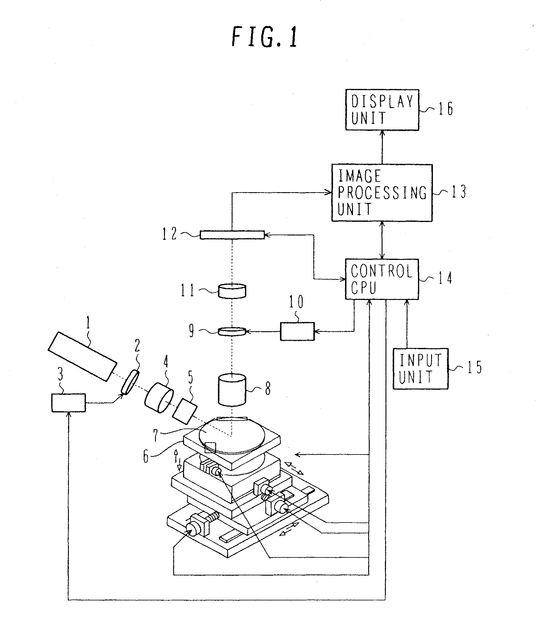
[0019]FIG. 1 is a schematic diagram illustrating the configuration of a defect inspection apparatus to which the present invention is applied. Referring to FIG. 1, a stage includes X, Y, Z, and θ (rotation) stages. A semiconductor wafer (specimen) 7, which is a typical inspection target pattern, is to be mounted on the stage 6. An illumination light source 1 is made of an ultraviolet or far-ultraviolet laser light source having a wavelength of 266 nm or 355 nm and used to illuminate the specimen 7.

[0020]The ultraviolet laser light source includes a device that uses a nonlinear optical crystal or the like, subjects a solid YAG laser to wavelength conversion, and generates a third harmonic (355 nm) or fourth harmonic (266 nm) of a fundamental wave. Alternatively, a laser light source having a wavelength of 193 nm, 195 nm, or 248 nm may be used. Another alternative is to use a l...


PUM

PropertyMeasurementUnit
wavelengthaaaaaaaaaa

Abstract

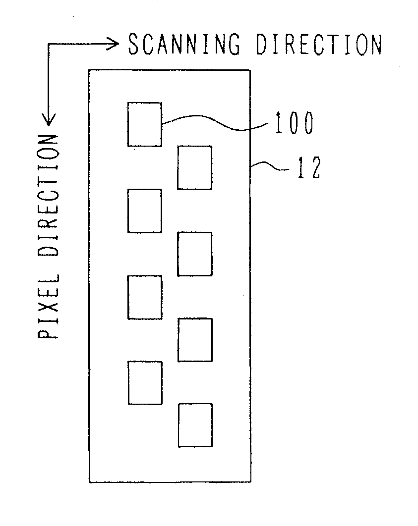
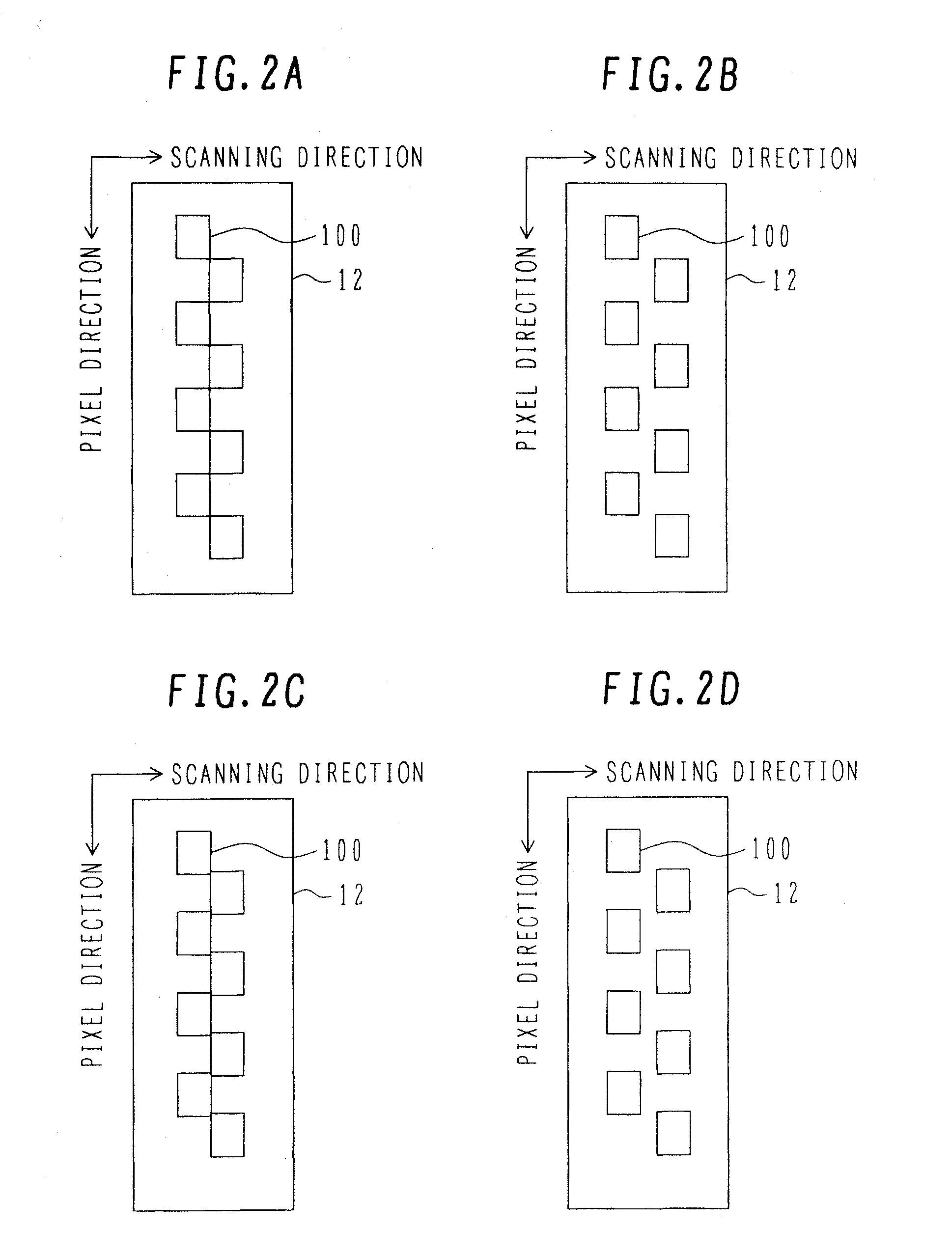
A high speed defect inspection apparatus has a high-speed detector that includes a plurality of image sensors. The image sensors are arranged with gaps between them in the pixel direction to form two lines. The image sensors are arranged in a zigzag pattern so that they are not contiguous to each other in the scanning direction. The development cost is reduced by using an arrangement of a plurality of small-area image sensors. When an image sensor is installed, it is necessary to furnish a region required for installation. Since individual image sensors need to be arranged at fixed intervals, void regions result. A plurality of image sensors are arranged in a zigzag pattern to solve the void region problem.

Description

BACKGROUND OF THE INVENTION[0001]1. Field of the Invention[0002]The present invention relates to a defect inspection apparatus that detects defects (e.g., shorts and wire breaks) and foreign matter in an inspection target pattern, and more particularly to a defect inspection apparatus that includes a plurality of photoelectric image sensors as a detector.[0003]2. Description of the Related Art[0004]In general, conventional methods for raising the inspection speed of a defect inspection apparatus have been used to increase the speed of an image sensor, which is employed as a detector. For example, the speed of an image sensor has been increased by the use of a method that divides the output of an image sensor having a large inspection field of view or a large number of pixels into even-numbered pixels and odd-numbered pixels and output the resulting pixels in a parallel manner or by the use of a so-called multi-tap output method, which divides all pixels of an image sensor into a plu...

Claims


Application Information

Patent Timeline
Patent Type & Authority Patents(United States)
IPC IPC(8): G01N21/00
CPCG01N21/8806G01N21/956G01R31/308
Inventor KAWAGUCHI, HIROSHI
Owner HITACHI HIGH-TECH CORP
Learn More