
Hot edge ring with sloped upper surface

a technology of sloped upper surface and hot edge ring, which is applied in the direction of coatings, chemical vapor deposition coatings, electric discharge tubes, etc., can solve the problems of significant erosion, corrosion and corrosion-erosion of the plasma-exposed surface of the processing chamber, and the plasma etch conditions create significant ion bombardment, corrosion and corrosion-erosion

Active Publication Date: 2011-12-27
LAM RES CORP
View PDF16 Cites 13 Cited by
  • Summary
  • Abstract
  • Description
  • Claims
  • Application Information

AI Technical Summary

Benefits of technology

[0007]The edge ring can be made of low-resistivity boron-doped single-crystalline silicon with...

Problems solved by technology

One challenge facing designers of plasma processing chambers is that the plasma etch conditions create significant ion bombardment of the surfaces of the processing chamber that are exposed to the plasma.
This ion bombardment, combined with plasma chemistries and / or etch byproducts, can produce significant erosion, corrosion and corrosion-erosion of the plasma-exposed surfaces of the processing chamber.
Another challenge is to control etch rate uniformity across a semiconductor substrate (e.g., silicon substrate), in particular, to make the etch rate at the center of the substrate equal to the etch rate at the edge.

Method used


Image

  • Hot edge ring with sloped upper surface
  • Hot edge ring with sloped upper surface
  • Hot edge ring with sloped upper surface

Examples


Embodiment Construction

[0016]As integrated circuit devices continue to shrink in both their physical size and their operating voltages, their associated manufacturing yields become more susceptible to particle and metallic impurity contamination. Consequently, fabricating integrated circuit devices having smaller physical sizes requires that the level of particulate and metal contamination be less than previously considered to be acceptable.

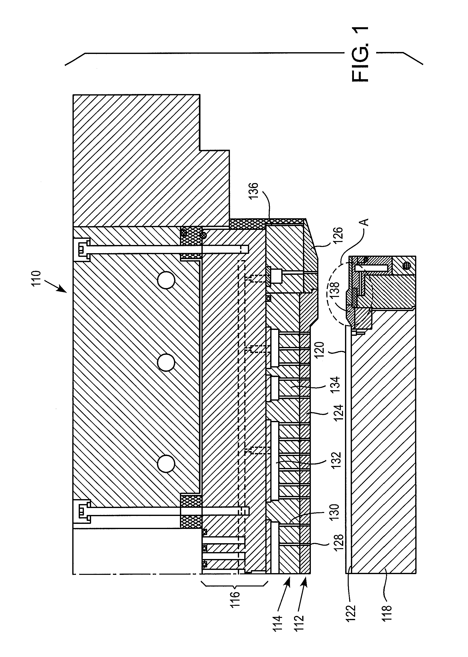
[0017]The manufacturing of the integrated circuit devices includes the use of plasma processing chambers. A plasma processing chamber may be configured to etch selected layers of a semiconductor substrate. Such a processing chamber is configured to receive process gases while a radio frequency (RF) power is applied to one or more electrodes in the processing chamber. The pressure inside the processing chamber is also controlled for the particular process. Upon applying the desired RF power to the electrode(s), the process gases in the chamber are activated such that a ...


PUM


Abstract

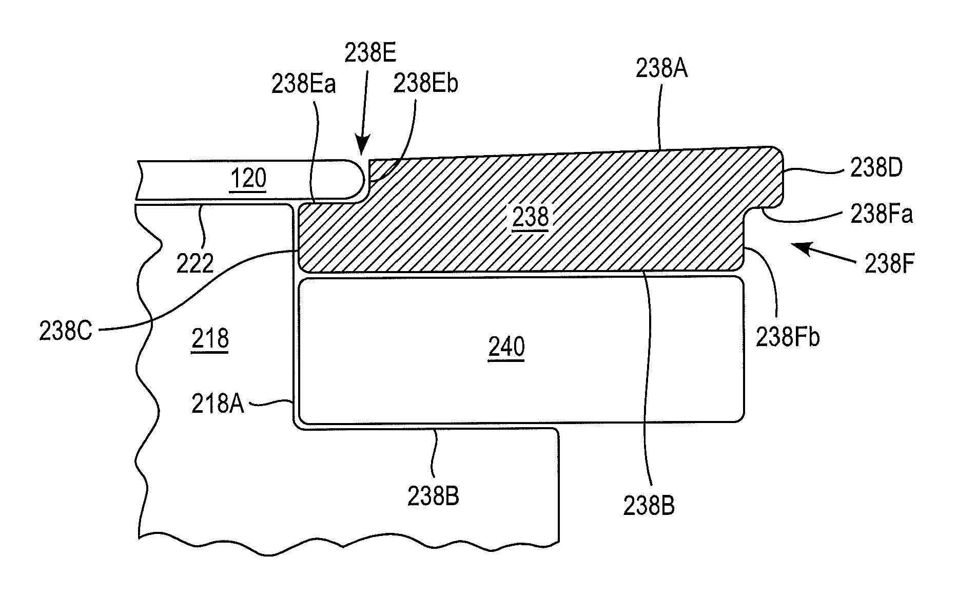
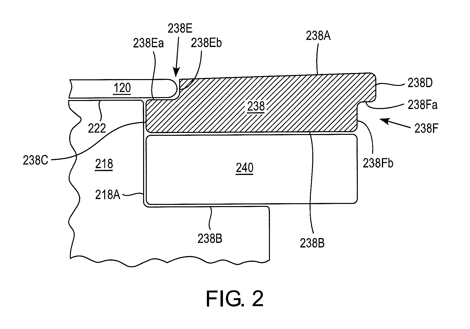
A hot edge ring with extended lifetime comprises an annular body having a sloped upper surface. The hot edge ring includes a step underlying an outer edge of a semiconductor substrate supported in a plasma processing chamber wherein plasma is used to process the substrate. The step includes a vertical surface which surrounds the outer edge of the substrate and the sloped upper surface extends upwardly and outwardly from the upper periphery of the vertical surface.

Description

[0001]This application claims priority under 35 U.S.C. §119 to U.S. Provisional Application No. 61 / 257,250 entitled HOT EDGE RING WITH SLOPED UPPER SURFACE, filed Nov. 2, 2009, the entire content of which is hereby incorporated by reference.BACKGROUND[0002]Plasma processing apparatuses are used to process semiconductor substrates by techniques including etching, physical vapor deposition (PVD), chemical vapor deposition (CVD), and resist removal. One type of plasma processing apparatus used in plasma processing includes a reaction chamber containing top and bottom electrodes. A radio frequency (RF) power is applied between the electrodes to excite a process gas into a plasma for processing semiconductor substrates in the reaction chamber.[0003]One challenge facing designers of plasma processing chambers is that the plasma etch conditions create significant ion bombardment of the surfaces of the processing chamber that are exposed to the plasma. This ion bombardment, combined with pl...

Claims


Application Information

Patent Timeline
IPC IPC(8): H01L21/00C23C16/00
CPCH01J37/20H01J37/317H01J37/32623H01J37/32091H01J2237/2001H01L21/68721H01L21/6875H01L21/68757G11B19/2009G11B33/148G11B5/5569
Inventor KOSHIISHI, AKIRAMANI, SATHYABHATTACHARYYA, GAUTAMBETTENCOURT, GREGORY R.CHAO, SANDY
Owner LAM RES CORP
Learn More