Structure and method for determining a defect in integrated circuit manufacturing process

a manufacturing process and integrated circuit technology, applied in semiconductor/solid-state device testing/measurement, semiconductor/solid-state device details, instruments, etc., can solve problems such as electrical shorts, defects that are difficult to detect for non-annealed polysilicon plugs, and defects that can be formed in pipes

Active Publication Date: 2012-01-03
ASML NETHERLANDS BV
View PDF12 Cites 87 Cited by
  • Summary
  • Abstract
  • Description
  • Claims
  • Application Information

AI Technical Summary

Problems solved by technology

In dynamic random access memory (DRAM) manufacturing, piping defects can be formed when there are voids or keyholes between word lines (WL) during inter-layer dielectric (ILD) deposition process.
Conducting material such as polysilicon that fills the contact holes also fills the voids or keyholes between the neighboring contact plugs in the ILD, which causes electrical short between neighboring contact plugs This defect is very difficult to detect for non-annealed polysilicon plugs.
Piping issue will become more challenging when DRAM feature size continues to shrink and the aspect ratio of the gap between WL becomes even larger.

Method used


Image

  • Structure and method for determining a defect in integrated circuit manufacturing process
  • Structure and method for determining a defect in integrated circuit manufacturing process
  • Structure and method for determining a defect in integrated circuit manufacturing process

Examples


Embodiment Construction

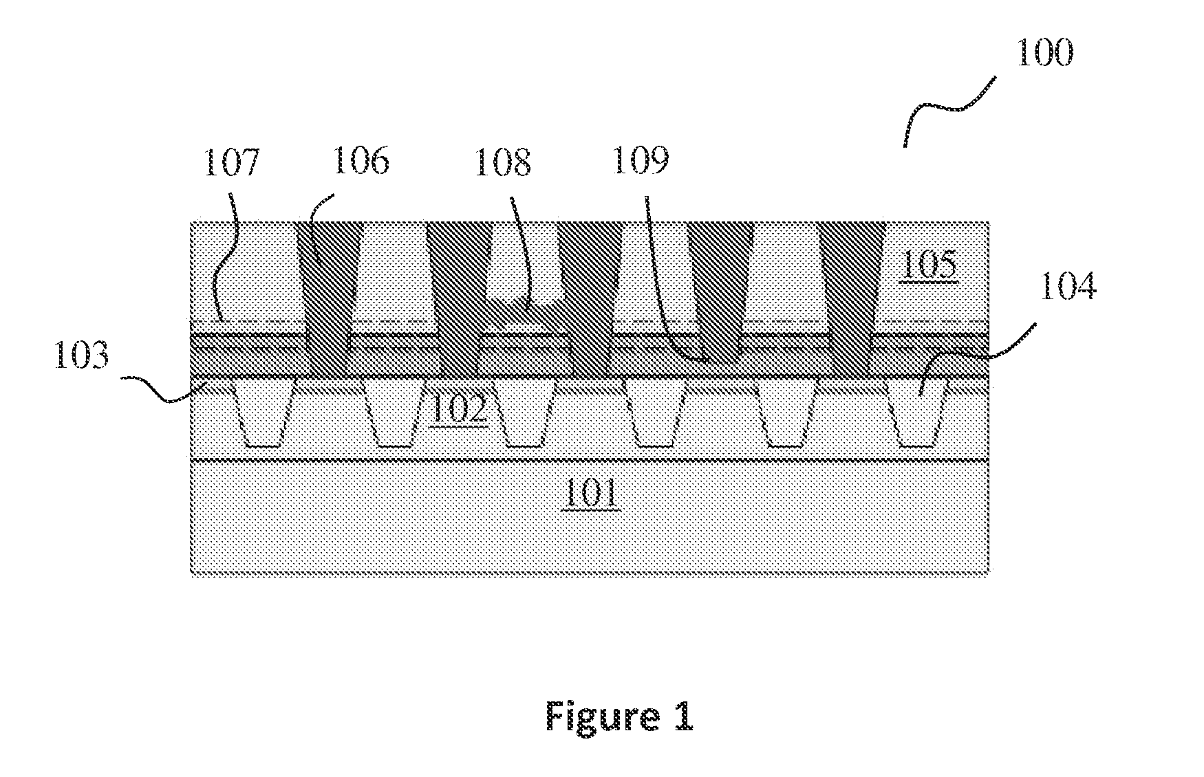
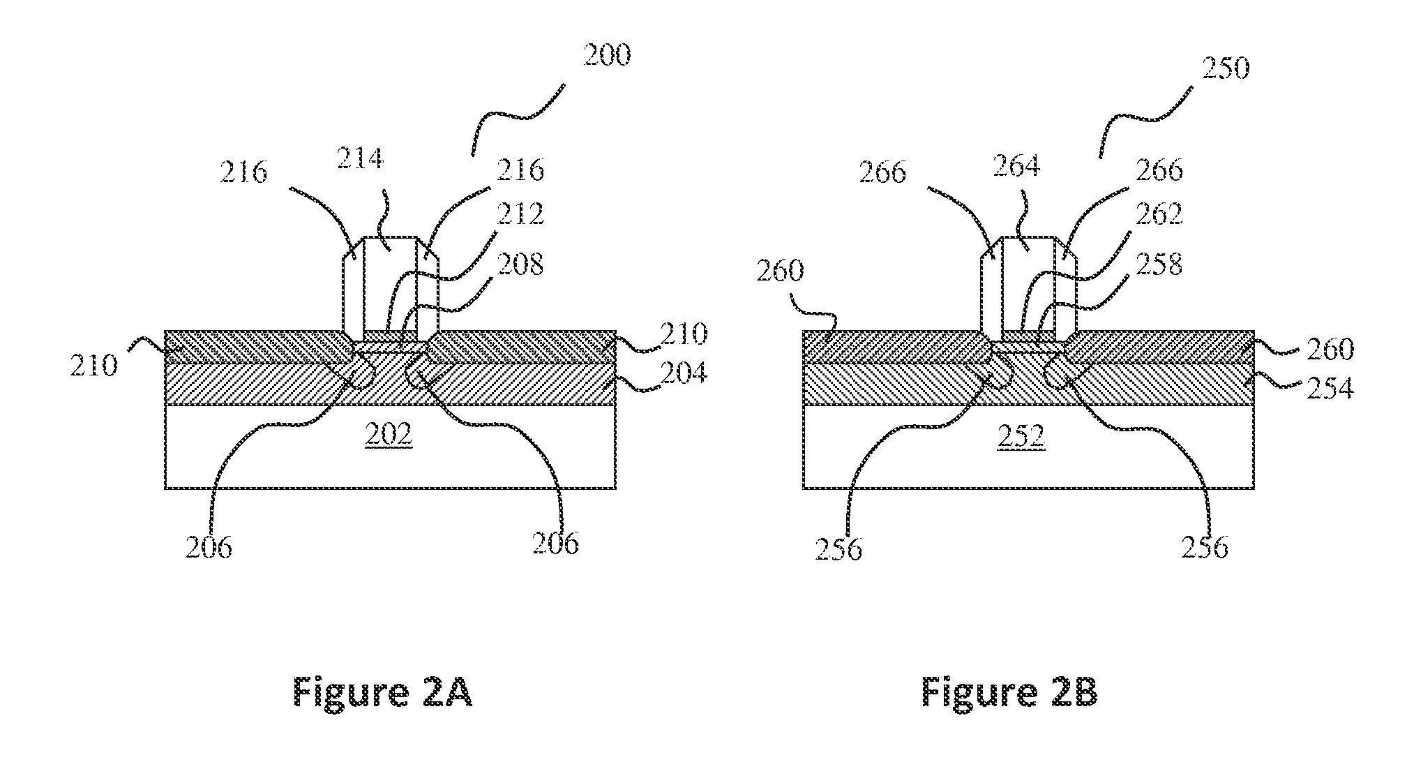
[0031]The present invention relates generally to the integrated circuit manufacturing process using a particle beam system. The following description is presented to enable one of ordinary skill in the art to make and use the invention and is provided in the context of a patent application and its requirements. Various modifications to the preferred embodiment and the generic principles and features described herein will be readily apparent to those skilled in the art. Thus, the present invention is not intended to be limited to the embodiment shown but is to be accorded the widest scope consistent with the principles and features described herein.

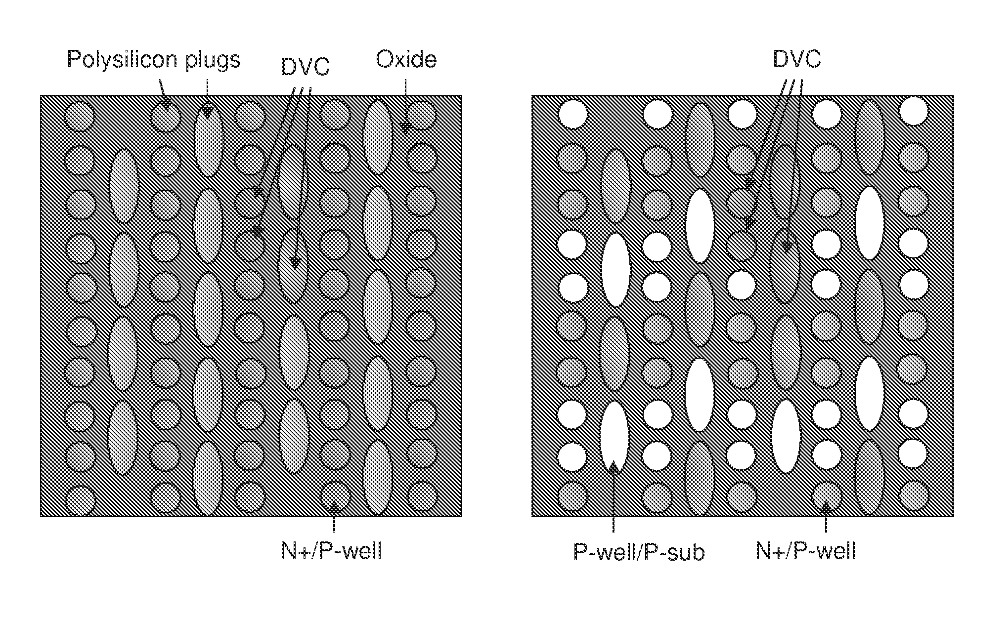
[0032]In a system and method in accordance with the present invention integrated circuit devices are designed to leak or short circuit by intentionally doping certain species in ion implantation processes that form wells, channels, source / drain (S / D) and pockets. These devices can then be used as a reference pattern for gray level measurem...


PUM


Abstract

The present invention discloses a structure and method for determining a defect in integrated circuit manufacturing process, wherein the structure comprises a plurality of normal active areas formed in a plurality of first arrays and a plurality of defective active areas formed in a plurality of second arrays. The first arrays and second arrays are interlaced, and the defect is determined by monitoring a voltage contrast from a charged particle microscope image of the active areas.

Description

CROSS-REFERENCE TO RELATED APPLICATIONS[0001]This Application is the U.S. Non-Provisional Patent application of U.S. Provisional Patent Application No. 60 / 914,020 filed on Apr. 25, 2007 entitled, “Test Structures For Manufacturing Process Monitoring Using Charged Particle Beam System” and U.S. Provisional Patent Application No. 60 / 940,165 filed on May 25, 2007 entitled, “Test Structures for Monitoring Electrical Short and Open Between Contact Plugs with Charged Particle Beam System” the priority of which is hereby claimed, and the entirety of which is incorporated herein by this reference.FIELD OF THE INVENTION[0002]The present invention relates generally to the integrated circuit manufacturing process using a particle beam system, in particular to a test structure and method for determining a defect in integrated circuit manufacturing process.BACKGROUND OF THE INVENTION[0003]Charged particle beam systems such as electron beam inspection (EBI) systems are increasingly applied in adv...

Claims


Application Information

Patent Timeline
Patent Type & Authority Patents(United States)
IPC IPC(8): G01R31/02G01R31/26
CPCH01L22/24H01L22/12
Inventor XIAO, HONGJAU, JACKYEH, CHANG CHUN
Owner ASML NETHERLANDS BV
Why Eureka
Try Eureka