Pattern forming method and apparatus, exposure method and apparatus, and device manufacturing method and device

a technology of exposure method and apparatus, which is applied in the direction of measurement devices, printers, instruments, etc., can solve the problems of reducing affecting the product quality of microdevices, and affecting the quality of exposure, so as to improve the productivity of microdevices with high integration and improve the productivity of microdevices. high integration

Active Publication Date: 2012-01-03
NIKON CORP
View PDF22 Cites 19 Cited by
  • Summary
  • Abstract
  • Description
  • Claims
  • Application Information

AI Technical Summary

Benefits of technology

[0011]With this method, during a period from the start of exposure to a plurality of pattern formation areas subject to exposure on the object until the end of the exposure, information on the positional relation between the energy beam and the object is detected by receiving the energy beam via the pattern forming apparatus, using the measurement pattern arranged on the movable body that holds the object. With this operation, even if the information on the positional relation between the energy beam and the object varies due to some reason, the variation can be detected during the period from the start to the end of the exposure to the plurality of pattern formation areas. Accordingly, by considering the detection results, as a consequence, high-precision exposure can be achieved.
[0029]Further, in a lithograph process, the productivity of microdevices with high integration can be improved by forming a pattern on an object and processing the object on which the pattern has been formed using any one of the first to third exposure methods of the present invention.

Problems solved by technology

However, in the scanning exposure apparatus that uses the micromirror array as the variable shaped mask, since it is relatively difficult to increase the size of the micromirror array, an illumination area (pattern formation area) on the substrate is so small (e.g. the width in a non-scanning direction (a direction orthogonal to a scanning direction in a plane parallel to the surface of the substrate) is about 0.2 mm).
Therefore, in the case of using a wafer with a diameter of 300 mm as the substrate, in order to expose one wafer (assuming that the entire surface of the wafer is exposed), the wafer needs to be scanned in the scanning direction at least about 1,500 times (750 round trips), which takes a long time.
Therefore, in the case of the scanning exposure apparatus of a maskless type, there is a possibility that temperature variation of the atmosphere in the vicinity of the substrate stage or the like occurs during exposure of one substrate, and due to the temperature variation, the measurement values of a measurement device (such as a laser interferometer) used for position measurement of the substrate stage vary, which causes measurement error.
In addition, there is also a risk that the exposure accuracy is lowered due to the measurement error.
Further, because the illumination area (pattern formation area) on the substrate is so small, it is difficult to expose a shot area with a size of 25 mm×33 mm on the wafer at one time.
When this method is employed for screen stitching in an exposure apparatus using a micromirror array, however, it is inefficient because some of micromirrors of the micromirror array are not used all through the exposure.

Method used


Image

  • Pattern forming method and apparatus, exposure method and apparatus, and device manufacturing method and device
  • Pattern forming method and apparatus, exposure method and apparatus, and device manufacturing method and device
  • Pattern forming method and apparatus, exposure method and apparatus, and device manufacturing method and device

Examples


first embodiment

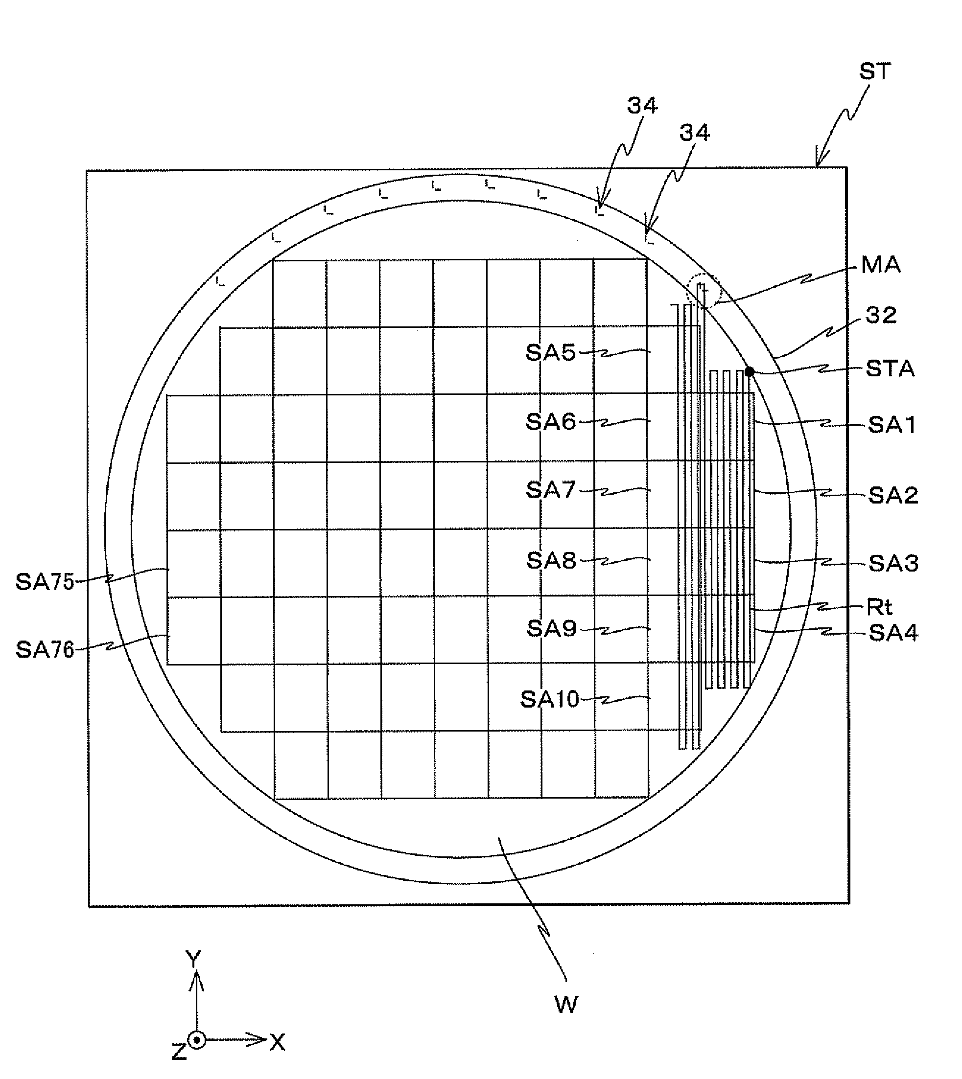
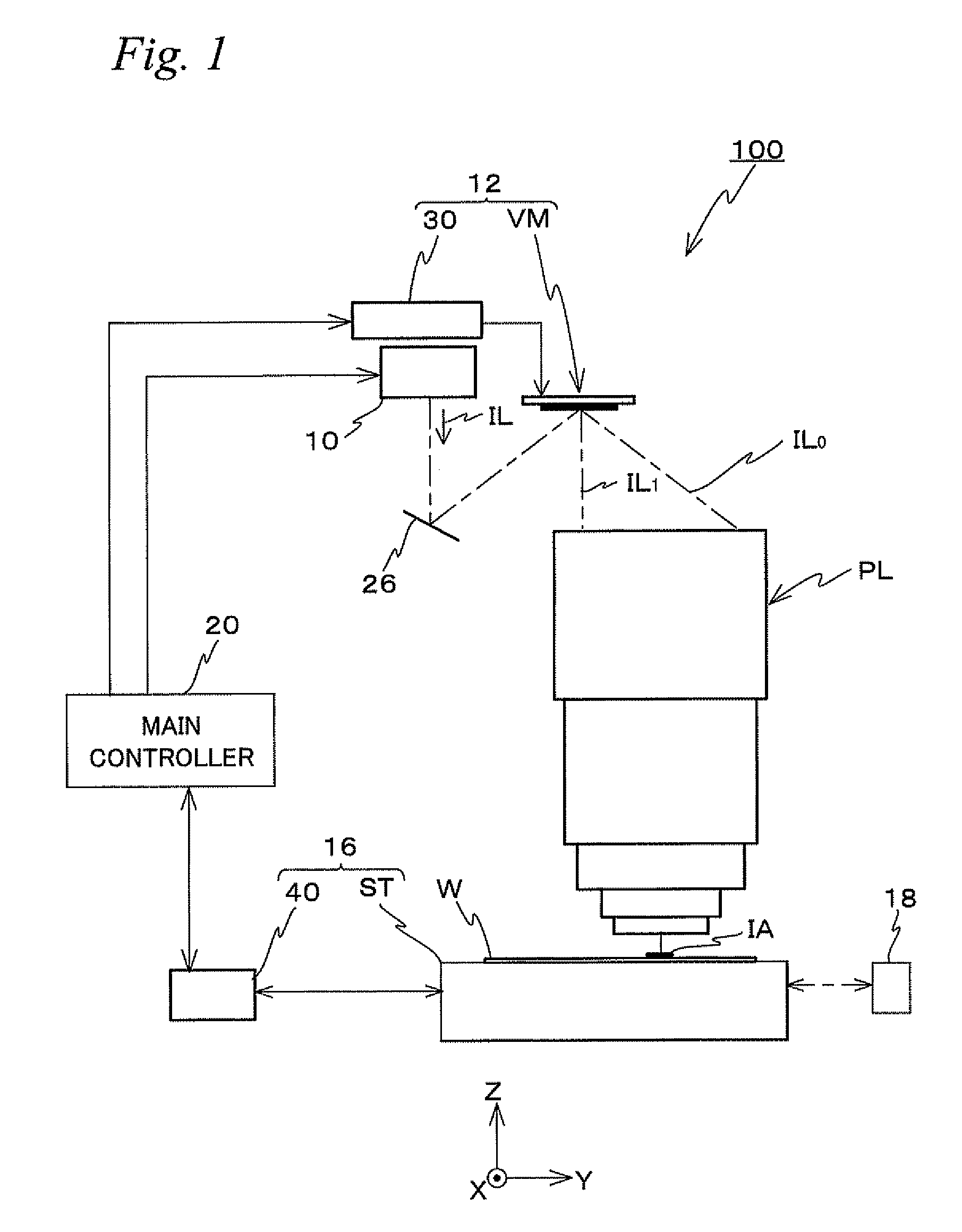
[0057]A first embodiment of the present invention is described below, referring to FIGS. 1 to 7. FIG. 1 schematically shows a configuration of an exposure apparatus 100 related to the first embodiment.

[0058]Exposure apparatus 100 is equipped with an illumination system 10, a pattern generating device 12, a projection optical system PL, a stage device 16, a control system, and the like. Exposure apparatus 100 forms an image of a pattern (a pattern image), generated by pattern generating device 12, on a wafer W mounted on a stage ST that constitutes a part of stage device 16, using projection optical system PL. The control system includes a microcomputer and is mainly configured of a main controller 20 that performs overall control of the entire apparatus. And, exposure apparatus 100 is a scanning type exposure apparatus that forms a pattern on wafer W by synchronizing change (switching) of generated patterns by a variable shaped mask VM and movement of wafer W.

[0059]Illumination syst...

second embodiment

[0118]A second embodiment of the present invention is described next, referring to FIGS. 9 and 22. Since an exposure apparatus related to the second embodiment has a configuration similar to that of the first embodiment described earlier, the same reference signs are used for the same or equivalent parts and the detailed description thereof is omitted herein, from the viewpoint of avoiding the redundant description. The exposure apparatus related to the second embodiment is different from that of the first embodiment in the point that main controller 20 computes control information with respect to drive system 30 in accordance with a pattern (a mask pattern) to be generated at variable shaped mask VM using templates (to be described later) in addition to the design data of a target pattern. In the description below, the different point from the first embodiment is mainly described.

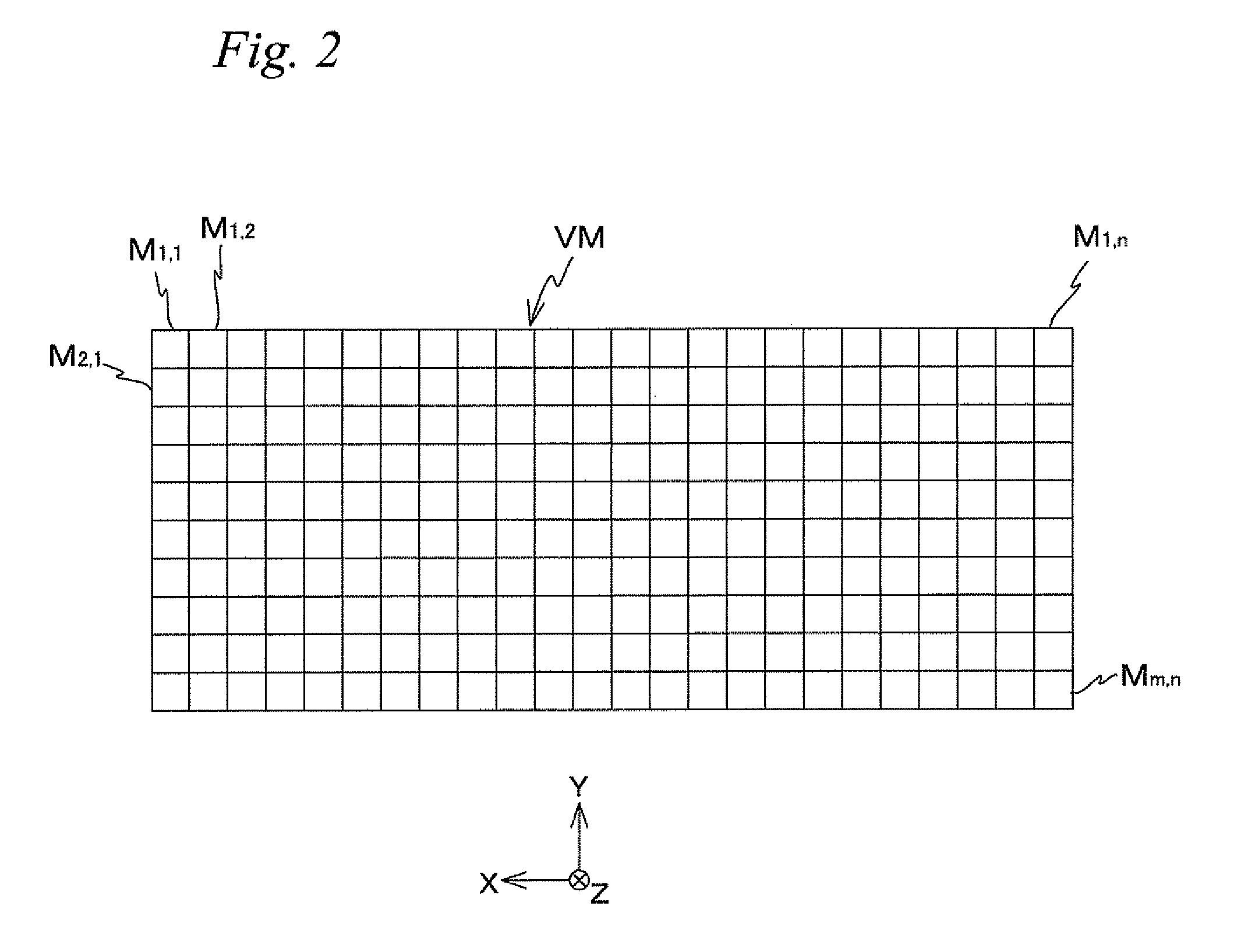
[0119]Now, the processing of forming a pattern image in a plurality of, for example, the K-number of sh...


PUM


Abstract

During a period after starting exposure to a plurality of shot areas subject to exposure on a wafer until completing the exposure, a light via a slit pair arranged on a stage that holds the wafer, of illumination light via a pattern generating device, is received, and information on a positional relation between an illumination light and the stage (and hence a positional relation between the illumination light and the wafer) is detected. With this operation, even if the information on the positional relation between the illumination light and the wafer varies due to some reason, information on the variation can be detected while performing the exposure to the plurality of shot areas. Accordingly, high-precision exposure can be achieved in an exposure operation, by considering this detection results.

Description

CROSS-REFERENCE TO RELATED APPLICATIONS[0001]This application is a continuation of International Application PCT / JP2008 / 001881, with an international filing date of Jul. 14, 2008, the disclosure of which is hereby incorporated herein by reference in its entirety, which was not published in English.BACKGROUND OF THE INVENTION[0002]1. Field of the Invention[0003]The present invention relates to pattern forming methods and apparatus, exposure methods and apparatus, and device manufacturing methods and devices, and more particularly, to a pattern forming method and a pattern forming apparatus to form a pattern in a divided area on an object using a variable shaped mask, an exposure method and an exposure apparatus to expose an object with an energy beam via the pattern forming apparatus, and a device manufacturing method using the pattern forming method or the exposure method, and a device manufactured with the device manufacturing method.[0004]2. Description of the Background Art[0005]...

Claims


Application Information

Patent Timeline
Patent Type & Authority Patents(United States)
IPC IPC(8): G03B27/32G01B11/00
CPCG03F7/70475G03F7/70291G03F9/7003G03F9/7015G03F9/7019
Inventor OWA, SOICHI
Owner NIKON CORP
Why Eureka
Try Eureka