Semiconductor switch and power conversion system provided with semiconductor switch

a technology of semiconductor switch and power conversion system, which is applied in the direction of pulse technique, process and machine control, instruments, etc., can solve the problems of increasing the scale of additional circuits, increasing the complexity of circuitry thereof, and increasing the size of auxiliary power supply having a relatively large capacity alkalis, so as to reduce the loss, simplify the circuit configuration, and effectively suppress the reverse recovery current of freewheel diodes

Active Publication Date: 2012-01-03
KK TOSHIBA
View PDF18 Cites 134 Cited by
  • Summary
  • Abstract
  • Description
  • Claims
  • Application Information

AI Technical Summary

Benefits of technology

[0004]The present invention has been accomplished in order to solve the above-described problems. It is therefore an object of the present invention to provide a semiconductor switch reduced further in loss and increased in switching speed by effectively suppressing the reverse recovery current of a freewheel diode, while simplifying a circuit configuration, and to provide a power conversion system applying the semiconductor switch.
[0018]According to the present invention, it is possible to more effectively suppress the reverse recovery current of a freewheel diode, while making a circuit configuration simpler in comparison with a conventional technology. Accordingly, it is possible to provide a semiconductor switch in which loss is further reduced, and a power conversion system applying the semiconductor switch. In addition, since the present invention is free from conventional constraints on switching timing, it is possible to provide a semiconductor switch having a switching speed higher than that in the conventional technology, and also provide a power conversion system applied with the semiconductor switch.

Problems solved by technology

However, in such a conventional power conversion system as disclosed in Patent Document 1 or Patent Document 2, a large current of a main circuit temporarily flows into an additional circuit at the time of reverse recovery of the freewheel diode, thus causing an increase in the scale of the additional circuit.
Consequently, the conventional power conversion system has a problem that a relatively large-capacity auxiliary power supply having a relatively large capacity alkalis required.
Accordingly, the conventional power conversion system provides a problem that the circuitry thereof becomes complicated.
This causes timing constraints to tighten and, therefore, makes the power conversion system unsuited for high-speed switching.

Method used


Image

  • Semiconductor switch and power conversion system provided with semiconductor switch
  • Semiconductor switch and power conversion system provided with semiconductor switch
  • Semiconductor switch and power conversion system provided with semiconductor switch

Examples


first embodiment

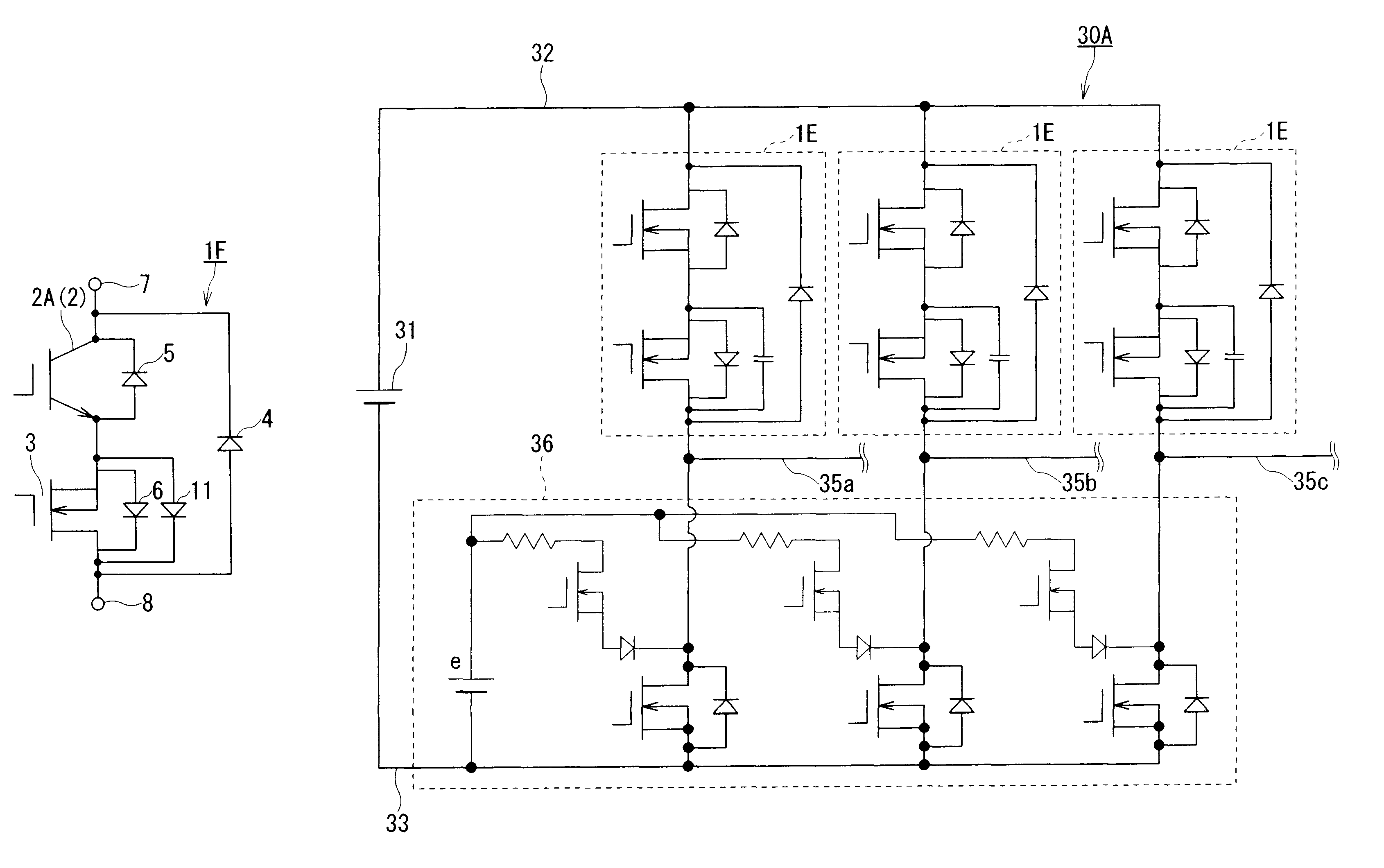
[0033]FIG. 1 is a circuit diagram illustrating a circuit configuration of a semiconductor switch 1A in accordance with a first embodiment of the present invention.

[0034]The semiconductor switch 1A is configured by connecting an auxiliary element 3 in series with a main element 2 serving as a switching element of a commonly-used power conversion circuit and by connecting a high-speed freewheel diode 4 having the same voltage resistance (withstand voltage) as that of the main element 2 in inverse parallel with the series connection of the main element 2 and the auxiliary element 3. That is, the semiconductor switch 1A is configured by adding an additional circuit comprising the auxiliary element 3 and the high-speed freewheel diode 4 to the main element 2.

[0035]The main element 2 of the semiconductor switch 1A is a highly voltage-resistant, voltage-driven element high in voltage resistance (withstand voltage) and an IGBT 2A containing a reverse-conducting diode 5, for example, is appl...

second embodiment

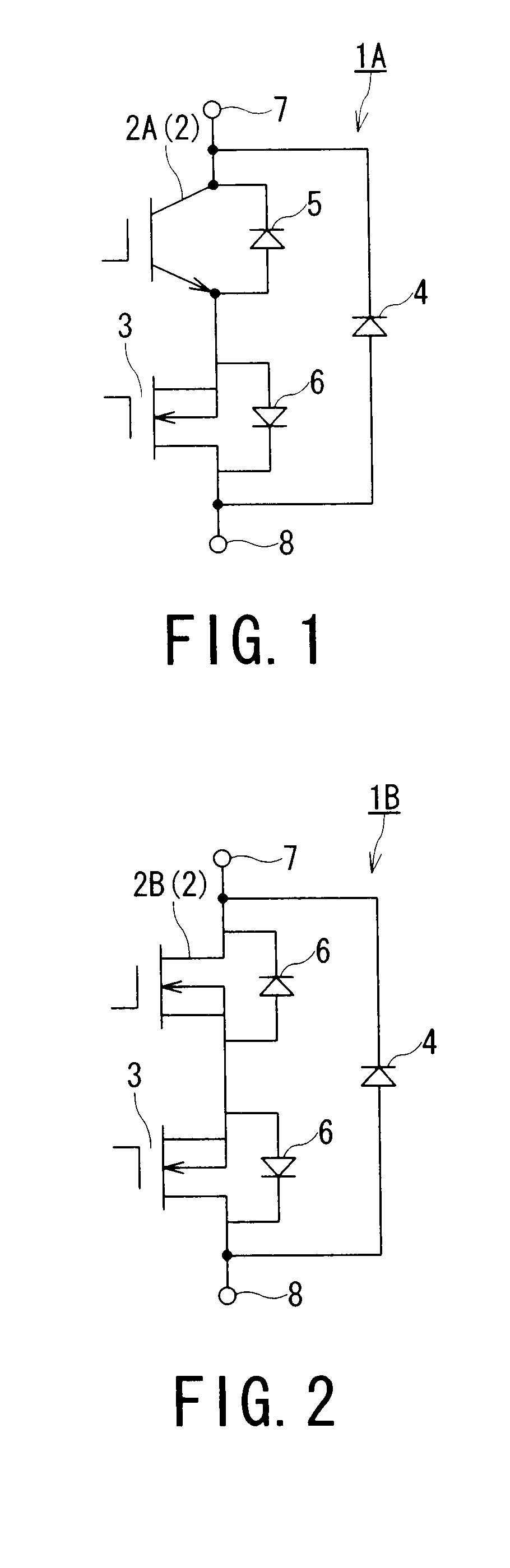
[0050]FIG. 2 is a circuit diagram illustrating a circuit configuration of a semiconductor switch 1B in accordance with a second embodiment of the present invention.

[0051]According to FIG. 2, the semiconductor switch 1B differs from the semiconductor switch 1A described in the first embodiment in that a MOSFET 2B is used for the main element 2 in place of the IGBT 2A. However, these semiconductor switches do not differ substantially in the rest of the configuration. Hence, components which do not substantially differ from those of the semiconductor switch 1A are denoted by like reference numerals and will not be explained again.

[0052]In cases where a MOSFET is applied as a main element, the reverse recovery characteristic of a reverse-conducting PN diode (parasitic diode), which is parasitically formed inside the MOSFET for reasons of the semiconductor structure of the MOSFET, becomes a problem. That is, there arises a problem that reverse recovery is extremely slow. In general, in o...

third embodiment

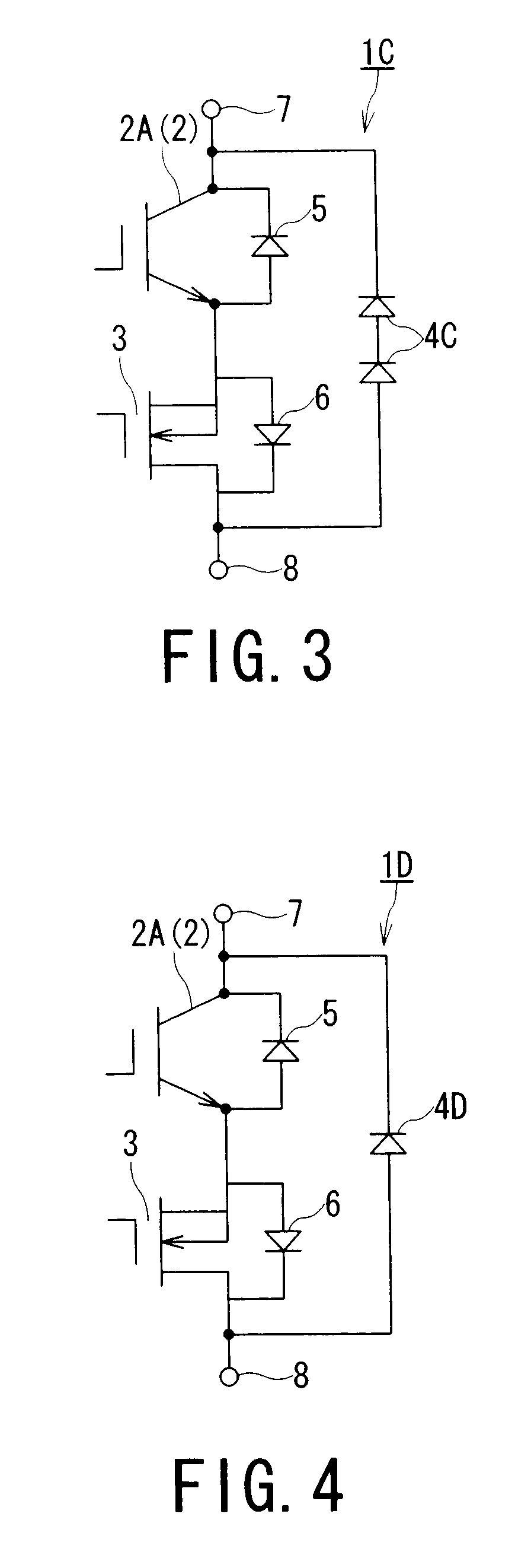
[0057]FIG. 3 is a circuit diagram illustrating a circuit configuration of a semiconductor switch 1C in accordance with a third embodiment of the present invention.

[0058]According to FIG. 3, the semiconductor switch 1C differs from the semiconductor switch 1A described in the first embodiment in that a plurality of high-speed freewheel diodes 4C (two in the example illustrated in FIG. 3) are used in place of the high-speed freewheel diode 4. However, these semiconductor switches do not differ substantially in the rest of the configuration. Hence, components which do not differ from those of the semiconductor switch 1A are denoted by like reference numerals and will not be explained again.

[0059]In general, the reverse recovery characteristic of a diode degrades with an increase in the withstand voltage thereof. Hence, the semiconductor switch 1C illustrated in FIG. 3 is configured by series-connecting two high-speed freewheel diodes 4C having a withstand voltage approximately half tha...


PUM


Abstract

A semiconductor switch is provided with a main element having reverse conductivity and serving as a voltage-driven switching element having a high withstand voltage, an auxiliary element serving as a voltage-driven switching element having a withstand voltage lower than that of the main element, and a high-speed freewheel diode having a withstand voltage equal to that of the main element, wherein a negative pole of the main element is connected to a negative pole of the auxiliary element to define the positive pole of the main element as a positive pole terminal and the positive pole of the auxiliary element as a negative pole terminal, and the high-speed freewheel diode is parallel-connected between the positive pole terminal and the negative pole terminal so that a direction from the negative pole terminal toward the positive pole terminal constitutes a forward direction.

Description

TECHNICAL FIELD[0001]The present invention relates to a semiconductor switch and a power conversion system and, more particularly, to a semiconductor switch for suppressing a reverse recovery current of a freewheel diode in a power conversion circuit having a configuration in which the freewheel diode is connected in inverse parallel with a main-circuit switching element, and also relates to a power conversion system applying the semiconductor switch.BACKGROUND ART[0002]Conventionally, as a power conversion circuit having a configuration in which a freewheel diode is connected in inverse parallel with a switching element in a main circuit, there has been proposed a power conversion circuit in which a loss caused as the result of the reverse recovery current of the freewheel diode being turned on is reduced. Such a power conversion system having a power conversion circuit is disclosed in, for example, Japanese Patent Laid-Open No. 2006-141167 (Patent Document 1) and Japanese Patent L...

Claims


Application Information

Patent Timeline
Patent Type & Authority Patents(United States)
IPC IPC(8): H02M3/335
CPCH02M1/08H02M7/5388H03K17/567H03K17/6874H01L2224/48137H01L2224/49111H01L2924/13055H01L2924/13091H01L2924/00H02M7/5387
Inventor MOCHIKAWA, HIROSHIKOYAMA, TATEOKUZUMAKI, ATSUHIKOTSUDA, JUNICHI
Owner KK TOSHIBA
Why Eureka
Try Eureka