Package of environmentally sensitive electronic device and fabricating method thereof

a technology packaging, which is applied in the direction of organic semiconductor devices, semiconductor devices, semiconductor/solid-state device details, etc., can solve the problems of large coefficient of thermal expansion, poor resistance to heat, moisture, oxygen and chemicals, and devices on these substrates experience accelerated aging, etc., to achieve the effect of prolonging the lifetime of environmentally sensitive electronic devices

Active Publication Date: 2012-01-10
HANNSTAR DISPLAY CORPORATION
View PDF17 Cites 29 Cited by
  • Summary
  • Abstract
  • Description
  • Claims
  • Application Information

AI Technical Summary

Benefits of technology

[0013]As aforementioned, the barrier structures are located between the first substrate and the second substrate, and the barrier structures surround the environmentally sensitive device. In addition, the water vapor transmission rate of the barrier structures is less than 10−1 g / m2 / day. Hence, the side wall barrier in the present invention protects well against water vapor and oxygen, and the package of the present invention prolongs the lifetime of the environmentally sensitive electronic device accordingly. Additionally, when the device is bent, the side wall barrier structures, acting as structural supports, disperse stress for the package of the environmentally sensitive electronic device.

Problems solved by technology

However, their drawbacks include a large coefficient of thermal expansion and poor resistance to heat, moisture, oxygen, and chemicals.
Since typical flexible substrates cannot entirely avoid the transmission of water vapor and oxygen, devices on these substrates experience accelerated aging.
Consequently, these devices with short lifetime fail to meet their commercial needs.
However, the capability of blocking water vapor and oxygen transmission of the mixed high viscoelastic glue and inorganic nano-materials is not as good as that of metallic layers having the stacking structure of multiple organic layers or multiple inorganic / organic layers.
In addition, the bonding reliability of the flexible optoelectronic device is worse.
Although this method is more conducive to water vapor and oxygen resistance than a conventional device, water vapor and oxygen still transmit into the device through the edge sealant, thereby shortening the lifetime of the device.
However, the water absorbing materials have a limited capability for the absorption of water vapor, and when such a capability is reached, water vapor enters the device region and affects the lifetime of the OLED.

Method used


Image

  • Package of environmentally sensitive electronic device and fabricating method thereof
  • Package of environmentally sensitive electronic device and fabricating method thereof
  • Package of environmentally sensitive electronic device and fabricating method thereof

Examples


Embodiment Construction

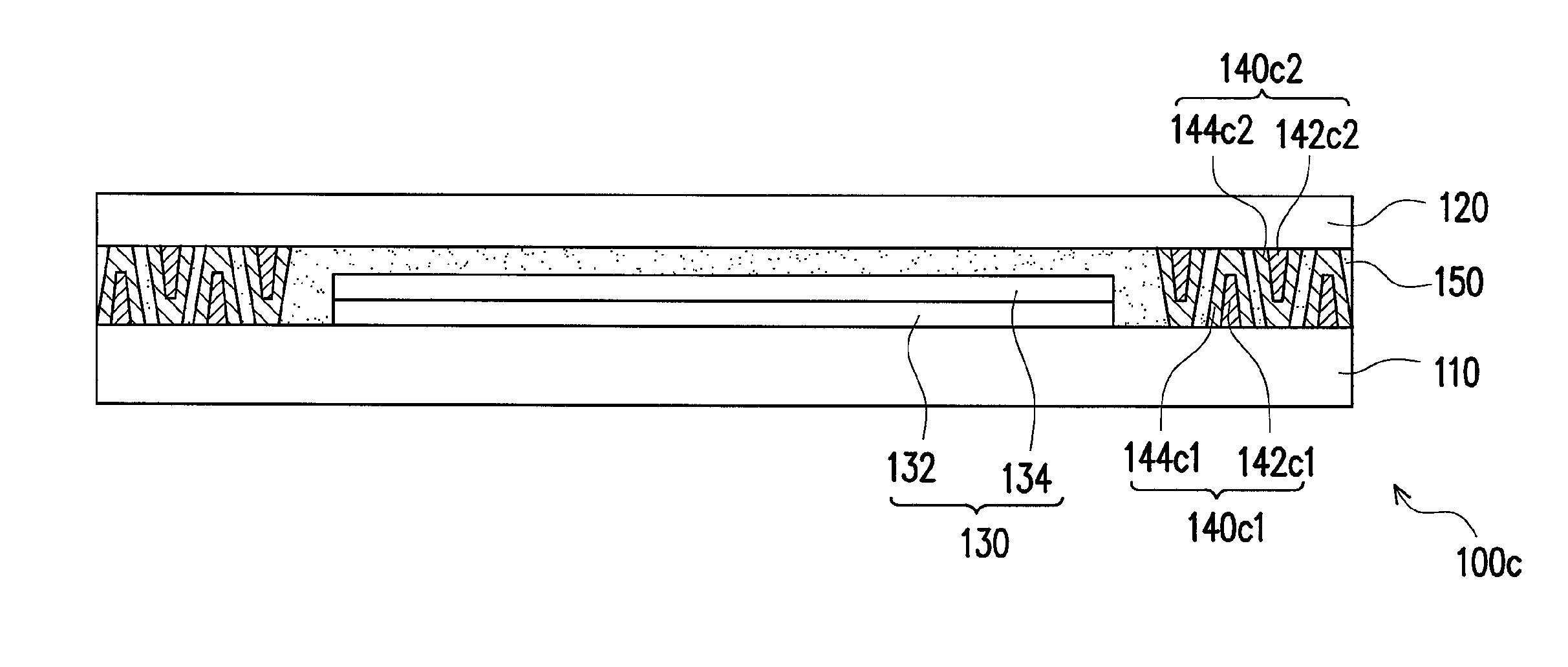
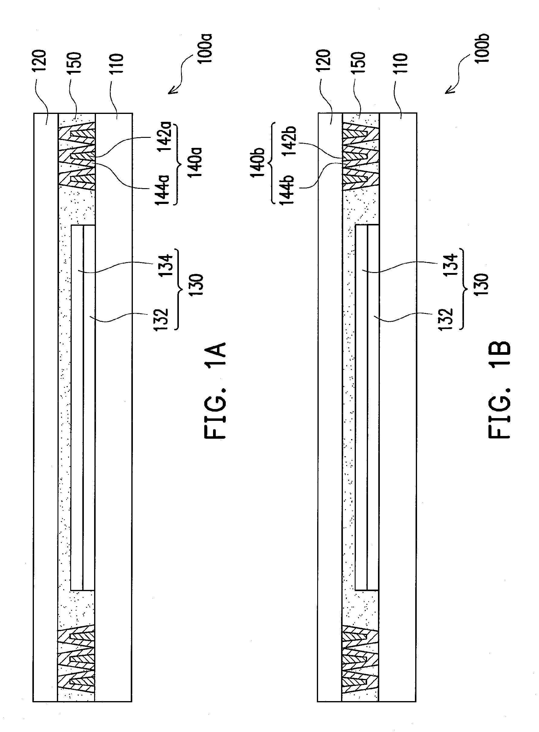
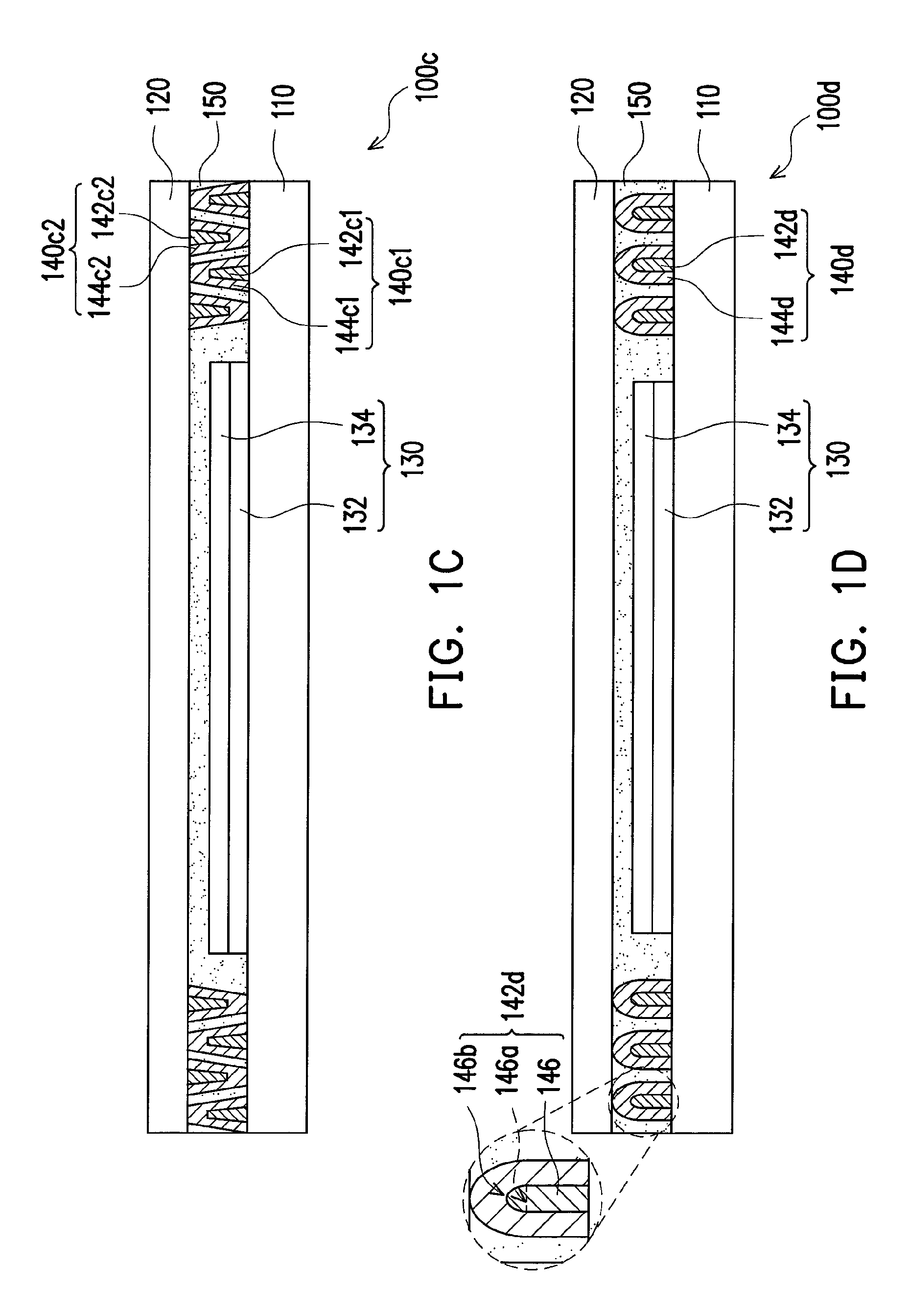
[0029]FIG. 1A is a schematic cross-sectional view of a package of an environmentally sensitive electronic device in accordance with one embodiment of the present invention. As shown in FIG. 1A, in the present embodiment of the invention, the package 100a having the environmentally sensitive electronic device includes a first substrate 110, a second substrate 120, an environmentally sensitive electronic device 130, a plurality of barrier structures 140a, and a fill 150.

[0030]Specifically, the second substrate 120 is disposed above the first substrate 110, and the first substrate 110 and the second substrate 120 can be a flexible substrate or a rigid substrate, for instance. A material for the flexible substrate is polyethylene terephthalate (PET), polyethylene naphthalate (PEN), polyethersulfone (PES), polymethylmathacrylate (PMMA), polycarbonate (PC), polyimide (PI), or metal foil. The flexible substrate can be a touch-sensing substrate. For instance, the flexible substrate 120 can ...


PUM

PropertyMeasurementUnit
water vapor transmission rateaaaaaaaaaa
metallicaaaaaaaaaa
flexibleaaaaaaaaaa

Abstract

A package of an environmentally sensitive electronic device including a first substrate, a second substrate, an environmentally sensitive electronic device, a plurality of barrier structures, and a fill is provided. The second substrate is disposed above the first substrate. The environmentally sensitive electronic device is disposed on the first substrate and located between the first substrate and the second substrate. The barrier structures are disposed between the first substrate and the second substrate, wherein the barrier structures surround the environmental sensitive electronic device, and the water vapor transmission rate of the barrier structures is less than 10−1 g / m2 / day. The fill is disposed between the first substrate and the second substrate and covers the environmentally sensitive electronic device and the barrier structures.

Description

CROSS-REFERENCE TO RELATED APPLICATION[0001]This application claims the priority benefit of Taiwan application Ser. No. 98112021, filed Apr. 10, 2009. The entirety of the above-mentioned patent application is hereby incorporated by reference herein and made a part of specification.BACKGROUND OF THE INVENTION[0002]1. Field of the Invention[0003]The present invention generally relates to a side wall barrier and a fabricating method thereof More particularly, the present invention relates to a side wall barrier of an environmentally sensitive electronic device and a fabricating method of an environmentally sensitive electronic device.[0004]2. Description of Related Art[0005]Compared with normal rigid substrates, flexible substrates have a wider range of applications due to their advantages of flexibility, ease of carriage, safety, and applications in consumer products. However, their drawbacks include a large coefficient of thermal expansion and poor resistance to heat, moisture, oxyge...

Claims


Application Information

Patent Timeline
Patent Type & Authority Patents(United States)
IPC IPC(8): H01L23/28
CPCH01L21/56H01L23/293H01L23/3121H01L23/564H01L51/5237Y10T29/49002H01L2924/12044H01L2924/0002H01L2251/5338H01L2924/00H10K50/8423H10K50/8428H10K50/8426H10K2102/311
Inventor CHEN, KUANG-JUNGHO, JIA-CHONGYAN, JING-YIYEH, SHU-TANG
Owner HANNSTAR DISPLAY CORPORATION
Why Eureka
Try Eureka