Thin film transistor substrate and a fabricating method thereof

a thin film transistor and substrate technology, applied in the direction of semiconductor/solid-state device manufacturing, semiconductor devices, electrical equipment, etc., can solve the problems of degrading one or more electrical properties of oxide semiconductor thin film transistors, poor uniform field effect mobility of commercially available polycrystalline silicon thin film transistors, and high cost of crystallization process equipment. achieve the effect of high productivity and reliability

Active Publication Date: 2012-01-17
SAMSUNG DISPLAY CO LTD
View PDF2 Cites 7 Cited by
  • Summary
  • Abstract
  • Description
  • Claims
  • Application Information

AI Technical Summary

Benefits of technology

[0009]Exemplary embodiments include an oxide semiconductor thin film transistor of high productivity and reliability, and a method of forming the same.

Problems solved by technology

A polycrystalline silicon thin film transistor can have acceptable field effect mobility, but a commercially available apparatus for the crystallization process is costly, and a uniformity of the field effect mobility of a commercially available polycrystalline silicon thin film transistor is poor due to the crystallization mechanism.
However, current processes, which are performed after disposing an oxide semiconductor, such as a plasma process or a wet process, or electrical stress, can degrade one or more electrical properties of the oxide semiconductor thin film transistor.

Method used


Image

  • Thin film transistor substrate and a fabricating method thereof
  • Thin film transistor substrate and a fabricating method thereof
  • Thin film transistor substrate and a fabricating method thereof

Examples


Embodiment Construction

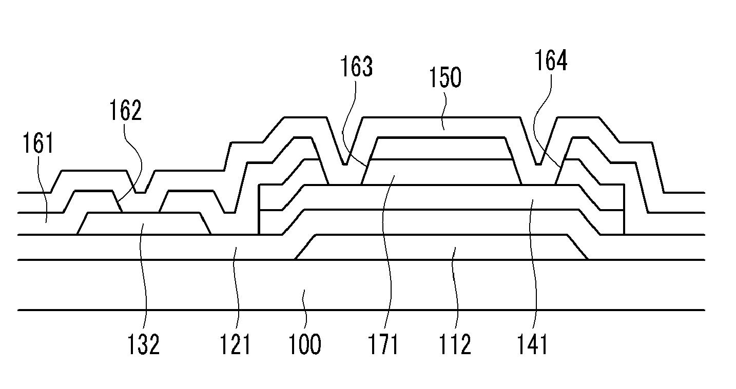
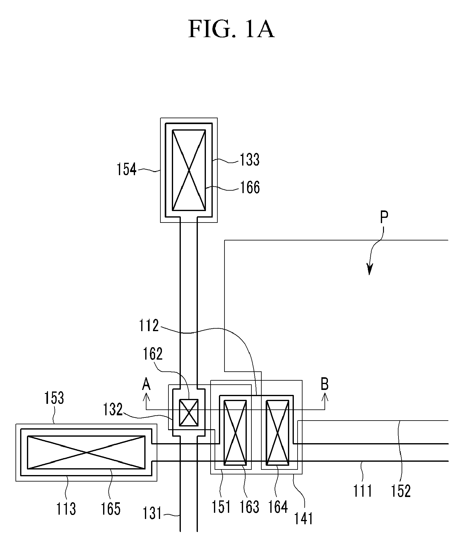
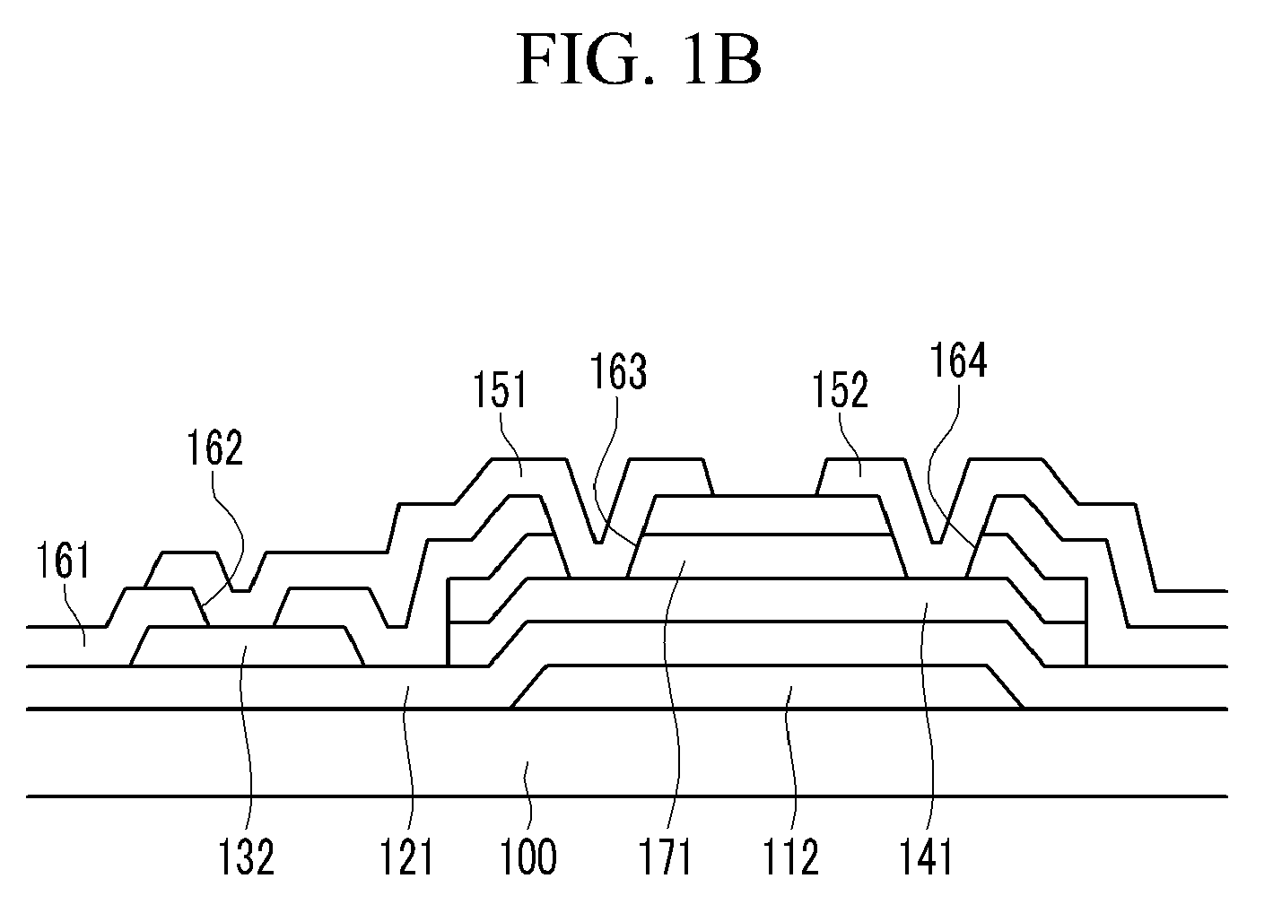
[0045]The invention is described more fully hereinafter with reference to the accompanying drawings, in which exemplary embodiments are shown. The invention may, however, be embodied in different forms and should not be construed as limited to the embodiments set forth herein. Rather, these embodiments are provided so that this disclosure will be thorough and complete, and will fully convey the scope of the invention to those skilled in the art.

[0046]In the figures, the dimensions of layers and regions may be exaggerated for clarity of illustration. It will also be understood that when a layer or element is referred to as being “on” another layer or element, it can be directly on the other layer or element, or intervening layers may also be present. Further, it will be understood that when a layer is referred to as being “under” another layer or element, it can be directly under, and one or more intervening layers or elements may also be present. In addition, it will also be underst...


PUM


Abstract

An oxide semiconductor thin film transistor substrate includes a gate line and a gate electrode disposed on an insulating substrate, an oxide semiconductor pattern disposed adjacent to the gate electrode, a data line electrically insulated from the gate line, the data line and the gate line defining a display region, a first opening exposing a surface of the data line, a second opening exposing a surface of the oxide semiconductor pattern, and a drain electrode disposed on the first opening and a drain electrode pad, the drain electrode extending from the first opening to the second opening and electrically connecting the drain electrode pad and the oxide semiconductor pattern.

Description

[0001]This application claims priority to Korean Patent Application No. 10-2008-0076813, filed on Aug. 6, 2008, and all the benefits accruing threrefrom under 35 U.S.C. §119, the contents of which in its entirety are herein incorporated by reference.BACKGROUND OF THE INVENTION[0002](1) Field of the Invention[0003]This disclosure relates to a thin film transistor substrate and a fabricating method thereof.[0004](2) Description of the Related Art[0005]Liquid crystal display (“LCD”) devices include a first substrate, which includes a thin film transistor (“TFT”), a second substrate disposed opposite the first substrate, and a liquid crystal layer interposed between the first and the second substrates. The liquid crystal layer may have anisotropic dielectric properties. LCDs can display images by adjusting the amount of light transmitted through the liquid crystal layer. The behavior of a liquid crystal layer can be controlled by a voltage difference applied to a common electrode and a ...

Claims


Application Information

Patent Timeline
Patent Type & Authority Patents(United States)
IPC IPC(8): H01L29/76H01L29/04H01L31/036H01L27/01H01L27/12
CPCH01L27/1225H01L29/7869G02F1/1368H01L27/124
Inventor LEE, YOUNG-WOOKYOO, HONG-SUKSONG, JEAN-HOYOUN, JAE-HYOUNGKIM, JONG-IN
Owner SAMSUNG DISPLAY CO LTD
Why Eureka
Try Eureka