Image recording material comprising electronic element

a technology of electronic elements and image recording materials, which is applied in the direction of photosensitive materials, auxiliaries/base layers of photosensitive materials, instruments, etc., can solve the problems of image non-uniformity, photographic paper peeling from the surface and no aforesaid patent publications have sufficiently studied the image quality formed in the image forming portion of the ic card

Inactive Publication Date: 2004-03-18
KONICA CORP
View PDF1 Cites 0 Cited by
  • Summary
  • Abstract
  • Description
  • Claims
  • Application Information

AI Technical Summary

Problems solved by technology

H11-11064, problems have occurred in which, during production of IC chip containing image forming materials employing injection molding, the aforesaid IC chip moves from the specified position due to action of resins injected into the die.
However, no aforesaid patent publications have sufficiently studied the image quality formed in the image forming portion on IC cards.
In the IC card described in JP-A No. 7-333783, which is prepared by adhering photographic paper, problems have been found in which image non-uniformity tends to occur.
Further, since the IC card disclosed in the aforesaid Patent Publication is structured by adhesion of photographic paper, problems have occurred in which when the card is repeatedly used or placed in the pocket of the bearer, the photographic paper peels from the surface of the IC card due to degrading of the adhesion surface caused by rep...

Method used


Image

  • Image recording material comprising electronic element
  • Image recording material comprising electronic element
  • Image recording material comprising electronic element

Examples


examples

[0100] The present invention will now be detailed with reference to examples. However, the embodiments of the present invention are not limited thereto.

first experiment

[0101] (First Experiment)

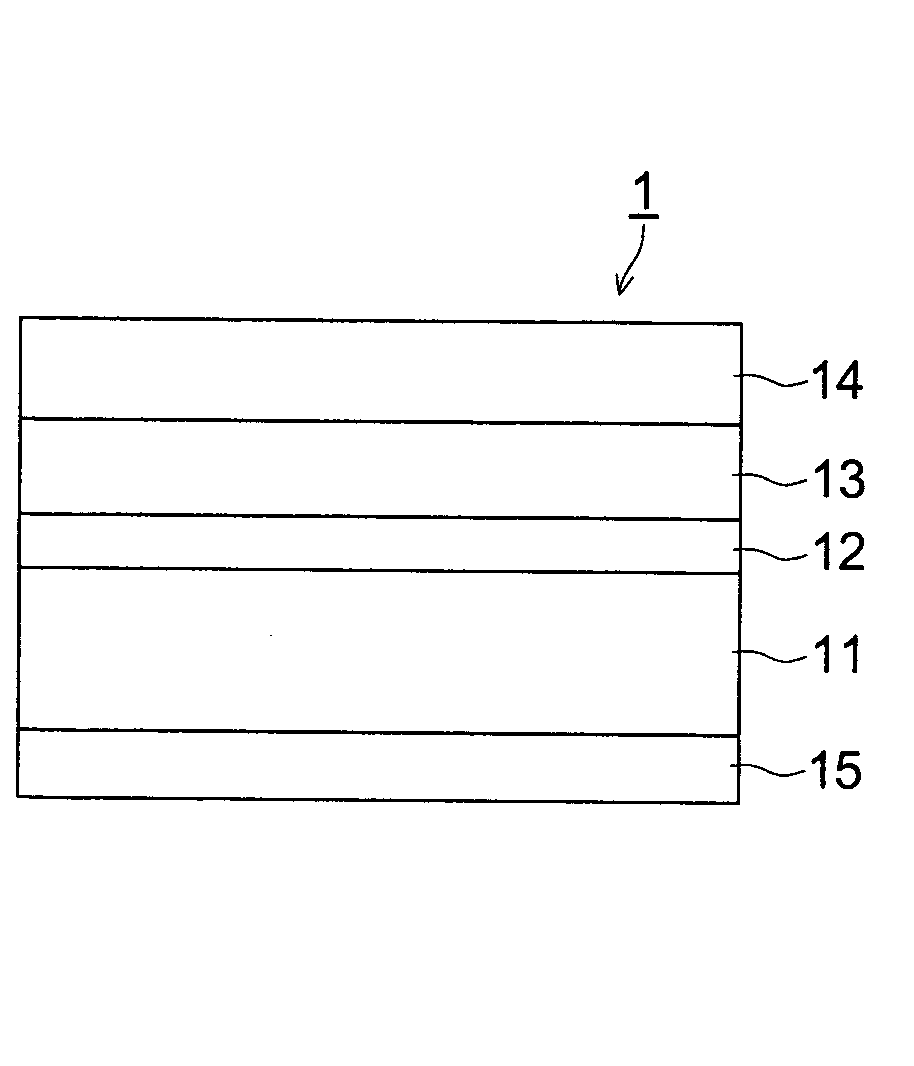
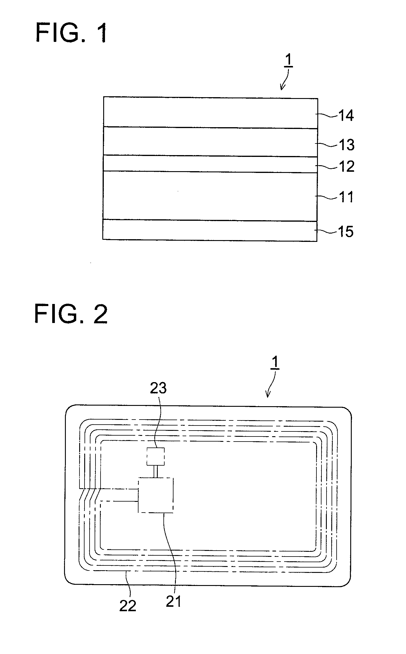
[0102] A substrate was prepared by laminating high-density polyethylene onto both surfaces of basis weight 180 g / m.sup.2 paper pulp, and a layer in which IC chips were to be installed was provided on the aforesaid support. Subsequently, on the aforesaid layer in which the IC chips were installed, were formed a white pigment containing-layer employing titanium oxide and an image forming layer. In such a manner, Examples 1-5, as well as Comparative Examples 1-6, were prepared which incorporated IC chip(s) installed in image recording materials in a credit card size, having a layer configuration shown in FIG. 1.

[0103] Incidentally, in Example 5, when the substrate was made, the IC chip is incorporated in the substrate by combining the fiber of the pulp with the electronic element, instead of preparing the electronic element layer containing the electronic element therein.

[0104] Further, the following data shown below were recorded in the IC chip employed in eac...

second experiment

[0114] (Second Experiment)

[0115] 1. Preparation of Example 6

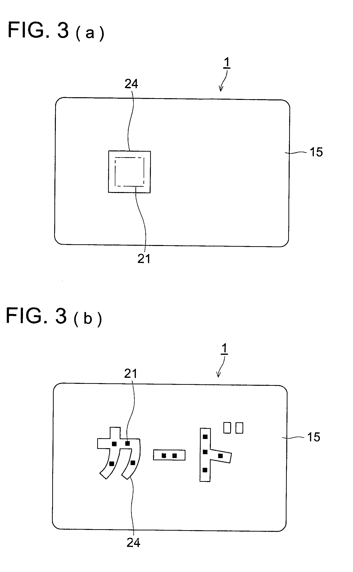
[0116] In this experiment, an image recording sheet (having a width of 200 mm and a length of 300 mm, on which IC chips were arranged at intervals of 64 mm across the width at 99 mm along the length) was employed which was Example 1 prepared in First Experiment and was capable of producing 9 cards in a credit card size (a width of 58 mm and a length of 85 mm) and which were in the pre-cutting stage. The word "TEST" was printed, employing a printing ink, on the printable layer provided on the support side opposite the image forming layer side of the aforesaid image recording sheet.

[0117] In such a case, printing was performed so that the central position (between letters E and S of "TEST") of the printed word matched to the arranged position of the built-in IC chip. Thereafter, the aforesaid sheet was cut to prepare 9 credit cared size samples, utilizing the central position of the printed word on the aforesaid sheet as a gu...


PUM


Abstract

An image recording material comprising: a substrate; an electronic element layer comprising an electronic element capable of radio communicating on the substrate; a white pigment-containing layer containing a white pigment on the electronic element layer; and an image forming layer on the white pigment-containing layer, herein, in the white pigment layer, a variation coefficient S/R of a ratio of a white pigment-occupying area per unit area is 0.25 or less, S is a standard deviation of the ratio and R is an average value of the ratio.

Description

[0001] The present invention relates to an image recording material, especially to an image recording material comprising an electronic element capable of radio communicating.TECHNICAL BACKGROUND[0002] Instead of conventional magnetic cards having magnetic stripes, IC cards having a larger memory capacity are utilized as an ID card for identification. The aforesaid IC card comprises IC chips (IC modules) in the card interior and is structured to make it possible to result in radio communication such as data transmitting and receiving with external instruments via electric contact points provided on the surface or a loop antenna in the card interior.[0003] Radio communication between the IC card and external instruments is achieved employing either a so-called contact type using electric contact points or a so-called non-contact type using an loop antenna installed in the card interior to send and receive signals.[0004] Incidentally, there are IC cards having an image forming surface...

Claims


Application Information

Patent Timeline
IPC IPC(8): G03C1/95G06K19/07G06K19/077B42D15/10
CPCG03C1/95
Inventor NISHIJIMA, TOYOKI
Owner KONICA CORP
Why Eureka
Try Eureka