

Semiconductor device
a semiconductor and semiconductor technology, applied in semiconductor devices, semiconductor/solid-state device details, electrical devices, etc., can solve the problems of initial separation and the likelihood of molding resin to separate achieve the effect of suppressing the separation of molding resin from the lead frame, easy disposal, and improved adhesion between the lead frame and the molding resin
- Summary
- Abstract
- Description
- Claims
- Application Information
AI Technical Summary
Benefits of technology
Problems solved by technology
Method used
Image

Examples
embodiment 1
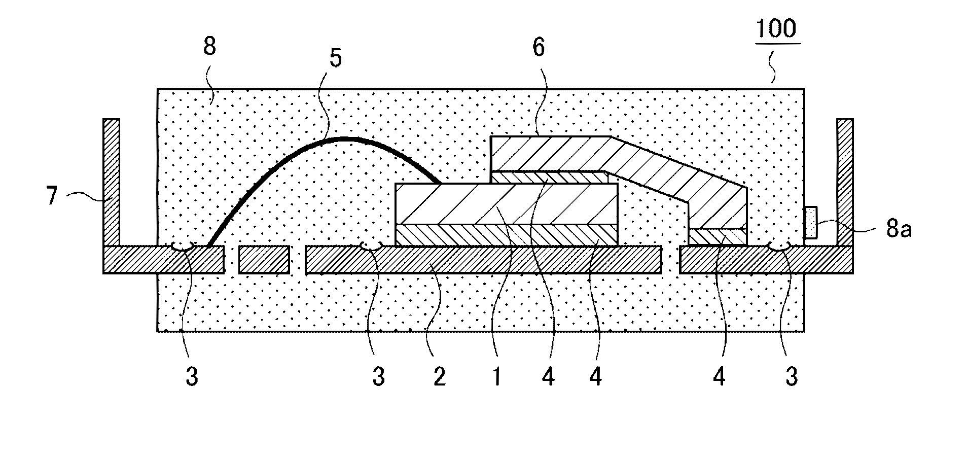
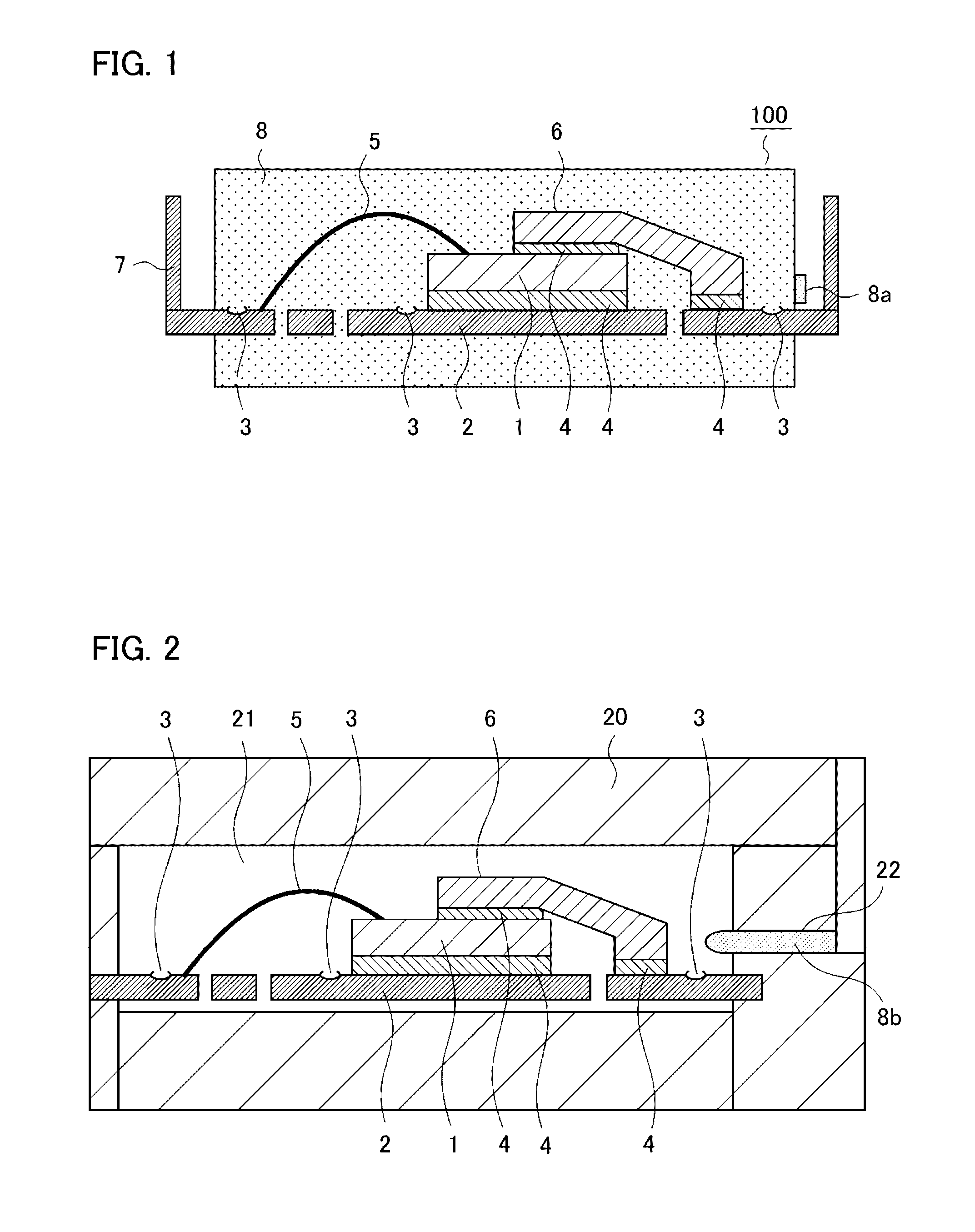
[0034]Hereafter, a description will be given, based on the drawings, of a semiconductor device according to Embodiment 1 of the invention. FIG. 1 shows an example of the structure of a resin molded semiconductor device according to Embodiment 1. A semiconductor device 100 according to Embodiment 1 is configured including a semiconductor element 1, a lead frame 2, a wire 5, an inner lead 6, an external terminal 7, and the like. In all the following drawings, identical and equivalent portions are given the same reference signs.
[0035]The semiconductor element 1 is, for example, an IGBT, a MOSFET, an IC chip, or an LSI chip, and is mounted on the top of the lead frame 2 via a joining member 4, such as solder or silver. The lead frame 2, on which to mount the semiconductor element 1 or other electronic components, is made of a copper plate or a copper alloy plate, and the front surface of the lead frame 2 is coated with metal plating (not shown), such as gold, silver, nickel, or tin. Als...
embodiment 2
[0065]As the overall configuration of a semiconductor device according to Embodiment 2 of the invention is the same as in Embodiment 1, the description of each portion will be omitted with FIG. 1 applied thereto. FIG. 15 is a top view showing a scale-like portion 3a in the semiconductor device 100 according to Embodiment 2, and FIG. 16 is a sectional view sectioned by the C-C portion shown in FIG. 15.
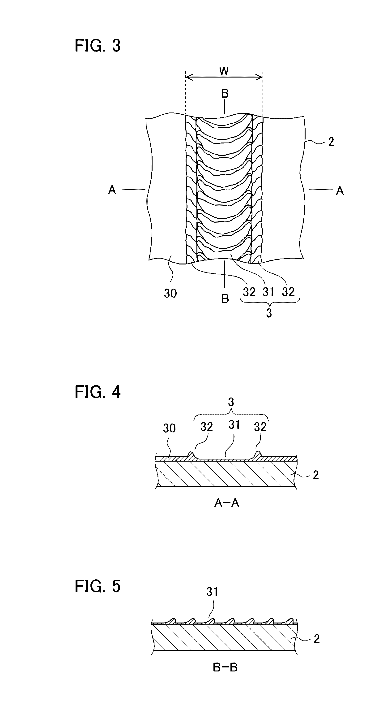
[0066]The scale-like portion 3a in Embodiment 2 has an exposed portion 2c which exposes the lead frame 2 underneath the metal plating layer 30, that is, copper or a copper alloy, in the vicinity of the central portion of the predetermined width W.
[0067]The other configurations are the same as those of the scale-like portion 3 in Embodiment 1. As the exposed copper or copper alloy has a high adhesion to the molding resin 8 compared with the metal plating layer 30, it is possible to more suppress the separation of the molding resin than in Embodiment 1.
[0068]As the method of exposing the ...
embodiment 3
[0071]In Embodiment 3 of the invention, a description will be given of an example wherein the scale-like portion 3 is applied to a semiconductor device different in configuration from the semiconductor device 100 according to Embodiment 1. FIG. 17 shows a semiconductor device 101 according to Embodiment 3. The semiconductor device 101 includes an electronic component 10 which is bridge mounted so as to bridge between two separated regions of the lead frame 2. The electronic component 10 is a capacitor, a thermistor, or the like.
[0072]In Embodiment 3, the two regions of the lead frame 2, in which the electronic component 10 is bridge mounted, may be a region in which the semiconductor element 1 is not mounted and a region in which the semiconductor element 1 is mounted, two regions in which the semiconductor element 1 is mounted, or two regions in which the semiconductor element 1 is not mounted.
[0073]When there is a distortion in the lead frame 2 when bridge mounting the electronic ...
PUM
 Abstract
Description
Claims
Application Information