System and method for data read of a synchronous serial interface NAND

a serial interface and data read technology, applied in the field of serial peripheral interfaces, can solve the problems of long erase and write time, no flash memory, and the nand flash memory typically requires some error detection and correction capabilities

Active Publication Date: 2012-01-24
MICRON TECH INC
View PDF10 Cites 31 Cited by
  • Summary
  • Abstract
  • Description
  • Claims
  • Application Information

AI Technical Summary

Problems solved by technology

However, a downside of NOR flash memory is that it experiences long erase and write times.
However, NAND flash memory typically requires some error detection and correction capabilities.
Moreover, NAND flash memory does not directly allow for random data access.
Due to the differences between NOR flash memory devices and NAND flash memory devices, a SPI system configured for use with a NOR flash memory device does not accommodate a NAND flash memory device.

Method used


Image

  • System and method for data read of a synchronous serial interface NAND
  • System and method for data read of a synchronous serial interface NAND
  • System and method for data read of a synchronous serial interface NAND

Examples


second embodiment

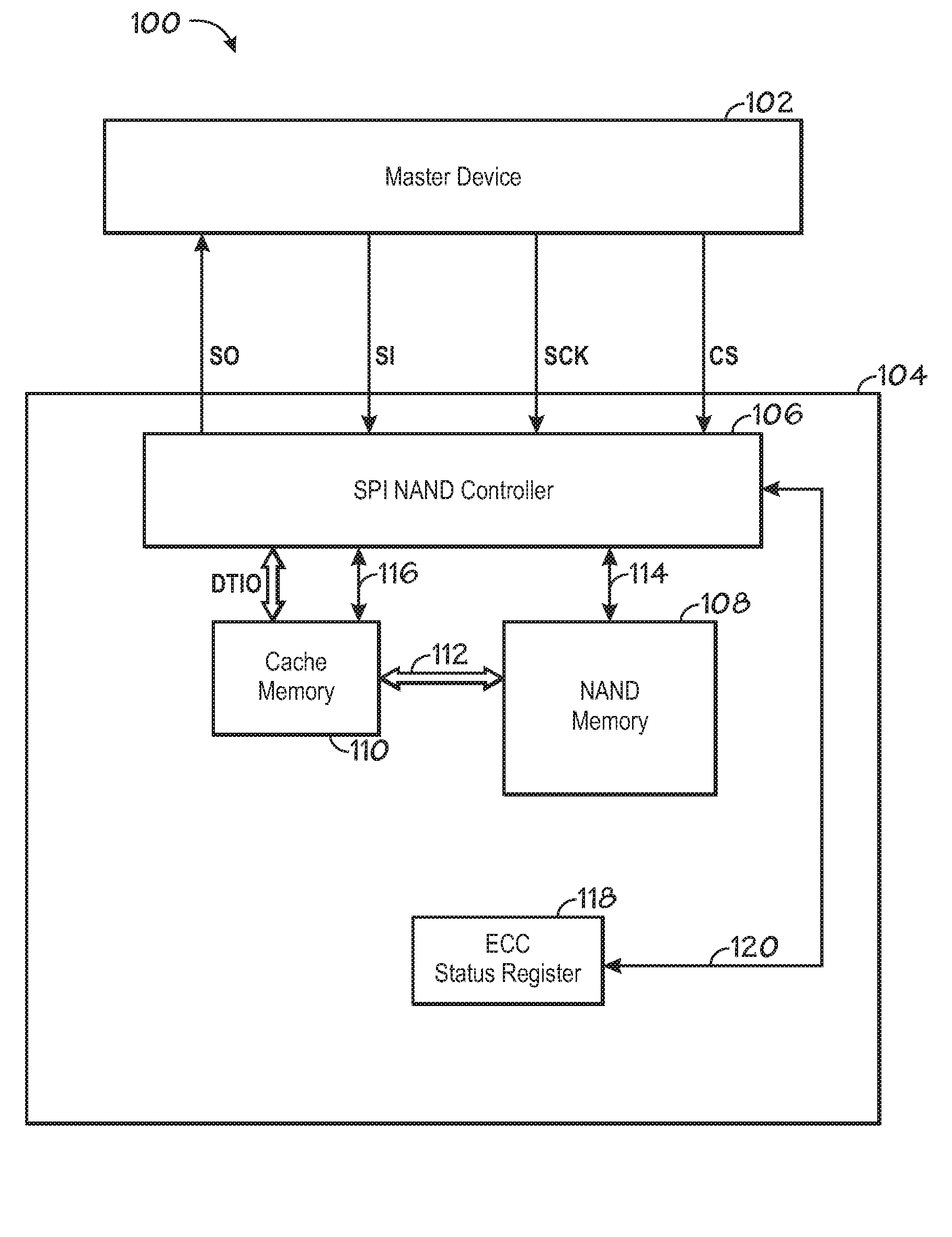
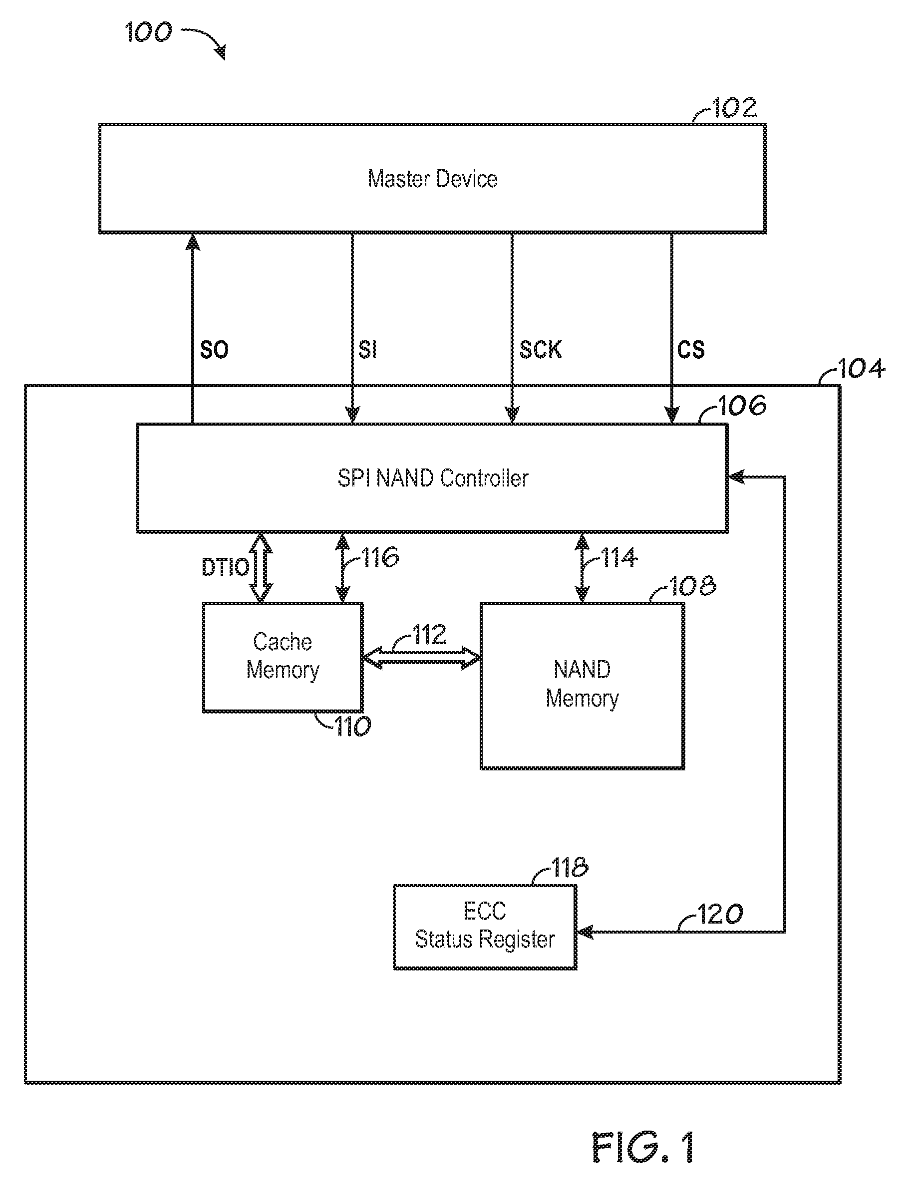
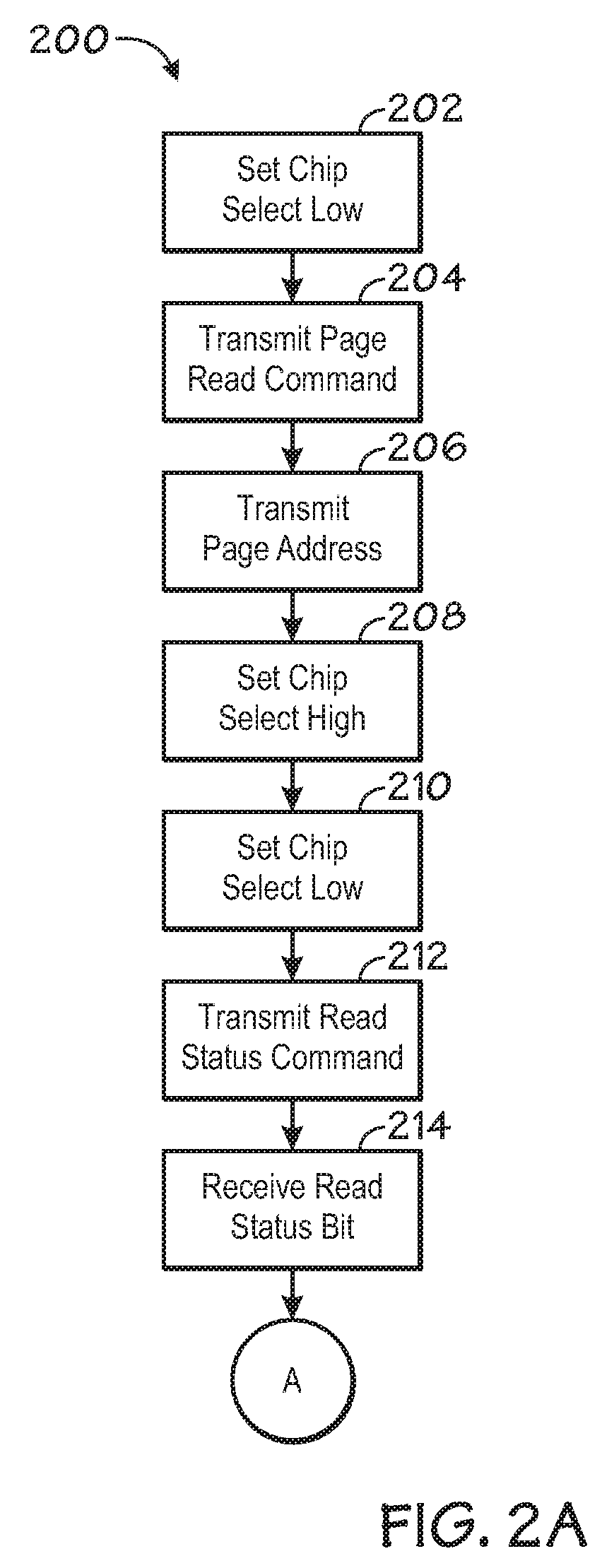
[0030]In FIG. 3, a flow chart illustrating the page read process 300 undertaken by the master device 102 to transmit a page read command to the slave device 104. At step 302, the CS is set to low by the master device 102, thus selecting the slave device 104 for information transmittal. In step 304, the master device 102 transmits a page read command to the slave device 104 on the SI line. The page read command operates to initialize the slave device 104 for a data read mode. Next, in step 306, the master device 102 transmits a page address to the slave device 104 across the SI line. In one embodiment, dummy bits may be transmitted as a header to the address transmitted to allow for proper byte alignment. For example, if a 17 bit row address is being transmitted, then a 7 dummy bit header may be transmitted so that the entire address length conforms to the slave device data input length requirements. Once the page address is transmitted, the master device 102 sets the CS value to hig...

third embodiment

[0036]In step 506, the SPI NAND controller 106 checks the data read in step 502 by implementing an error detection process. The error detection process uses the redundancy bits corresponding to the data in detecting any errors in the data. If any errors are found, then they are corrected in step 508 using the ECC process. In one embodiment, the error detection and correction techniques make use of linear block encoding and decoding. A further embodiment utilizes specialized subclasses of binary BCH codes, such as Hamming codes to perform the error detection and correction. A third embodiment utilizes nonbinary BCH codes, such as Reed-Solomon codes to perform the error detection and correction of the data. Upon completion of steps 506 and 508, the data is sent across access line 116.

[0037]In step 510, the ECC result register 118 is updated. Preferably, the ECC status register 118 includes sub-registers used to store error detection and correction result information. In one embodiment...


PUM


Abstract

A method and system is disclosed for operating a NAND memory device. The NAND memory device is operated by transmitting serial peripheral interface signals from a host to a NAND memory device, whereby the signals are communicated to a NAND memory in the NAND memory device without modifying the signals into a standard NAND memory format. Similarly, a method and system is disclosed for receiving signals from the NAND memory device without modifying the signals from a standard NAND format into a serial format. The system also incorporates error detection and correction techniques to detect and correct errors in data stored in the NAND memory device.

Description

BACKGROUND[0001]1. Field of the Invention[0002]Embodiments of the invention relate generally to a Serial Peripheral Interface for connecting a host device to memory devices.[0003]2. Description of the Related Art[0004]A serial peripheral interface bus (SPI) is a four wire serial communication interface that enables a serial data link between two devices, a master and a slave. It provides support for a low to medium bandwidth network connection between the devices supporting the SPI. Since SPI utilizes only four wires for communication, SPI has become popular for use in systems that require relatively simple IC packages.[0005]The four wires of the SPI include of two control lines and two data lines. The control lines of the SPI include a Chip Select (CS) line and a Serial Clock (SCK) line. While more than one slave device can be connected to the master device, only one slave device may be accessed at any given time. This selection is accomplished by use of the CS line. A CS signal is...

Claims


Application Information

Patent Timeline
Patent Type & Authority Patents(United States)
IPC IPC(8): G11C29/00
CPCG06F13/4291G11C16/26G06F11/1064G06F3/0679G06F11/1068G06F3/0619G06F3/0629G11C7/1006G11C2207/104G11C2207/2245G11C2216/30
Inventor PEKNY, THEODORE T.TSAI, VICTOR Y.FEELEY, PETER S.
Owner MICRON TECH INC
Why Eureka
Try Eureka